Solid-state imaging device and method for producing the same

a solid-state imaging and imaging method technology, applied in the direction of radio-controlled devices, instruments, television systems, etc., can solve the problems of deterioration of transfer efficiency and sensitivity reduction, affecting the production efficiency of solid-state imaging, and reducing the resolution limit of fine patterns, etc., to achieve high withstand voltage, high reliability of solid-state imaging, and easy production

Inactive Publication Date: 2007-02-15
FUJIFILM CORP
View PDF14 Cites 45 Cited by
  • Summary
  • Abstract
  • Description
  • Claims
  • Application Information

AI Technical Summary

Benefits of technology

[0041] According to the present invention, the gate oxide film is composed of a two-layer film consisting of a silicon oxide film and a metal oxide thin film, so that even when the gate oxide film does not contain a silicon nitride film, high wit

Problems solved by technology

However, in order to form a thin and good-quality oxide film, the oxidation temperature needs to be high of 900° C. or more as described above and impurity diffusion on the substrate side proceeds due to heat history by oxidation, incurring various problems such as deterioration of transfer efficiency and reduction of sensitivity.
In this way, the formation of an interelectrode insulating film by using thermal oxidation is a big obstacle standing in the way of developing a fine (high-quality) solid-state imaging device with a large number of pixels.
In the case of a charge transfer electrode having a single-layer electrode structure,

Method used


Image

  • Solid-state imaging device and method for producing the same
  • Solid-state imaging device and method for producing the same
  • Solid-state imaging device and method for producing the same

Examples


embodiment 1

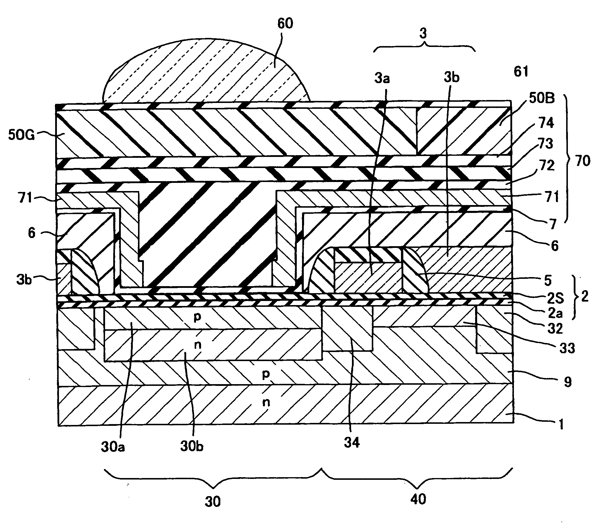
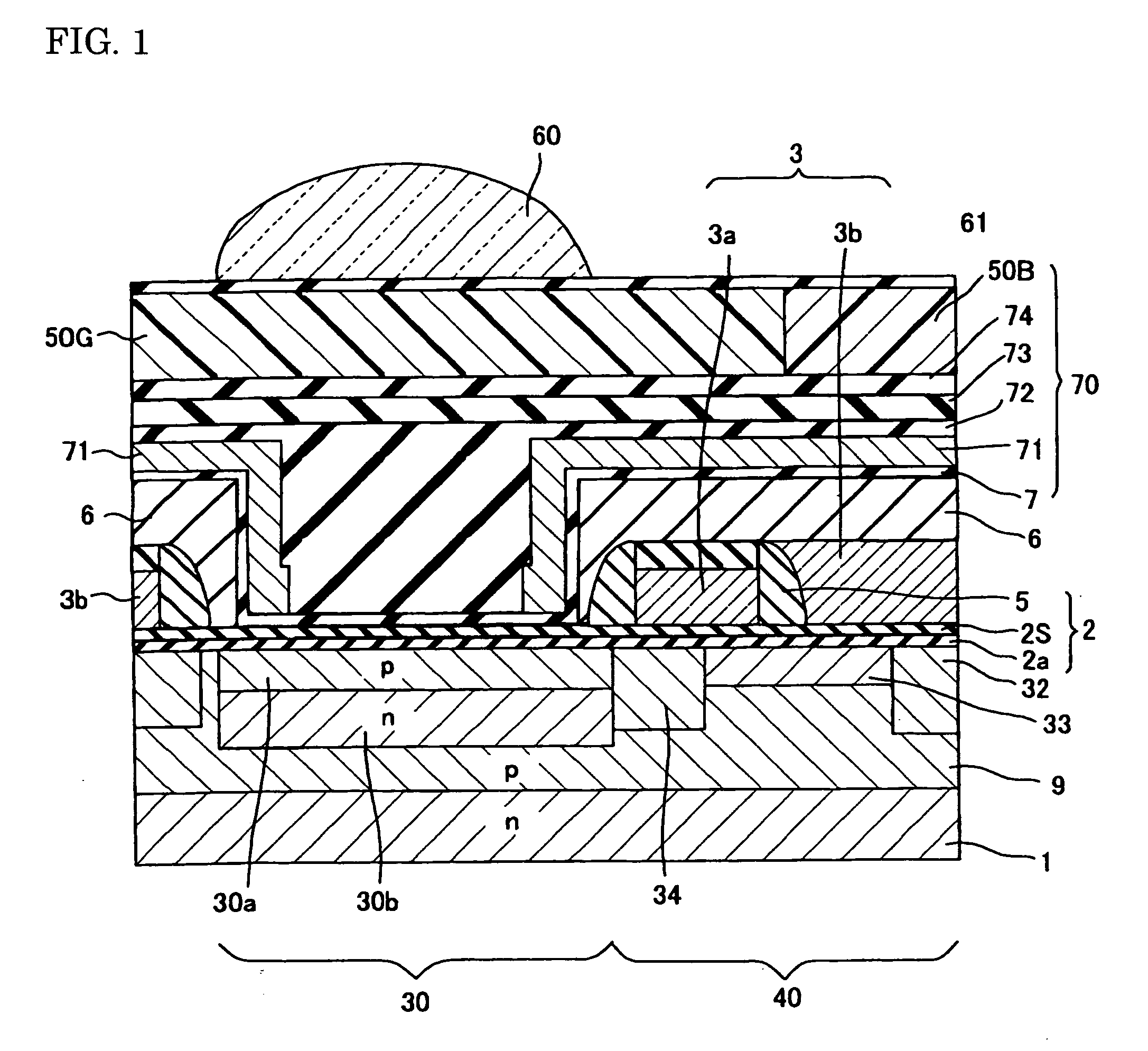
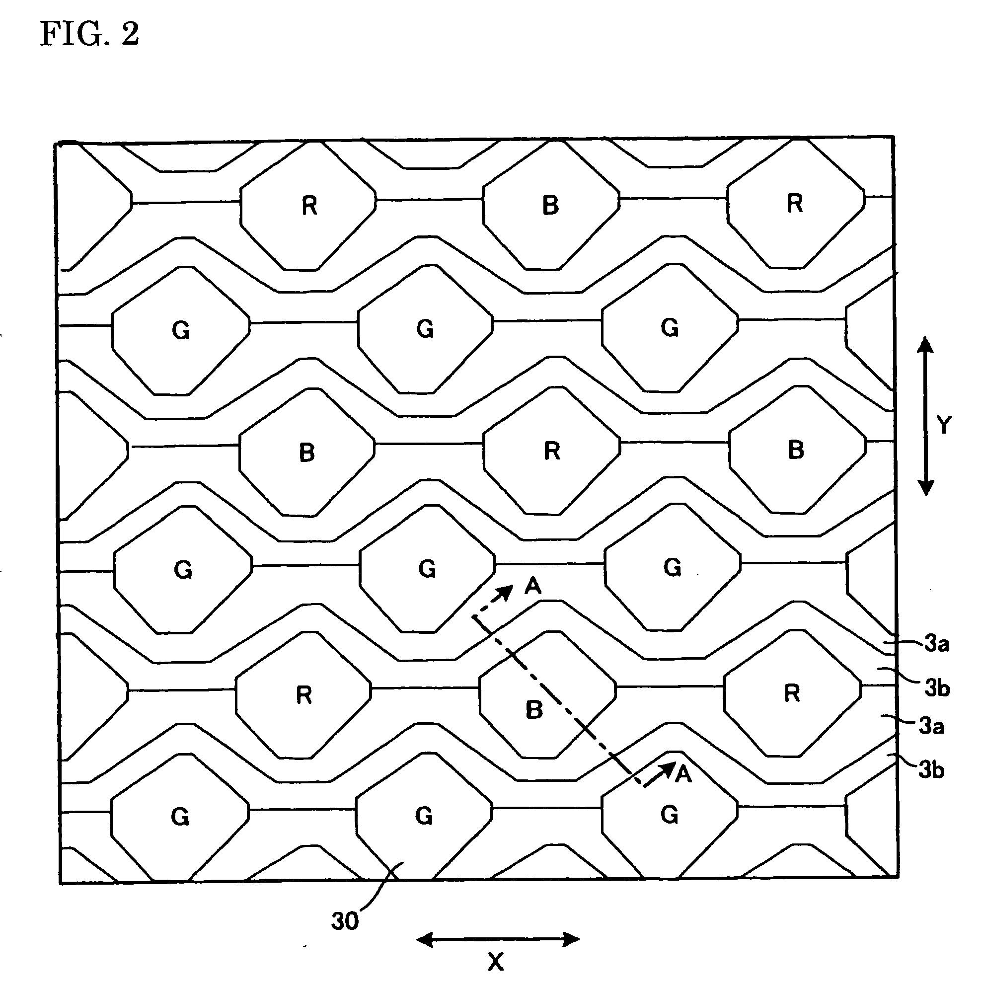
[0049] This solid-state imaging device is characterized in that, as illustrated in FIGS. 1 and 2, the gate oxide film 2 comprises a two-layer film consisting of a silicon oxide film 2a and a hafnium oxide layer 2S. This hafnium oxide layer 2S has a role of acting as an etching stopper layer in the anisotropic etching process at the formation of a sidewall insulating film and at the same time, preventing charge trapping. Although the solid-state imaging device has the structure of a normal solid-state imaging device except for this, a first layer electrode 3a comprising a polycrystalline silicon layer as the first layer electrically conducting film and a second layer electrode 3b comprising a polycrystalline silicon layer as the second layer electrically conducting film are alternately juxtaposed on the gate oxide film 2, and the interelectrode insulating film is composed of a sidewall insulating film 5 comprising an HTO film (silicon oxide film) formed by a CVD process. The numeral ...

embodiment 2

[0075] In Embodiment 1, a laminate film consisting of a silicon oxide film and a hafnium oxide layer is used as the gate oxide film, but in place of the high dielectric thin film such as hafnium oxide layer, a low dielectric thin film having etching resistance may be used at the etching of silicon oxide.

[0076] According to this constitution, a thin and highly reliable gate oxide film can be formed because of its high etching selectivity and low dielectric constant, so that finer fabrication can be attained.

embodiment 3

[0077] The patterning of the first layer electrode sometimes brings about film loss of the gate oxide film, but in this Embodiment, the film loss may be supplemented by forming the silicon oxide film by a CVD process.

[0078] In the Embodiments above, a charge transfer electrode having a single-layer electrode structure is described, but the same is applicable also to a charge transfer electrode having a two-layer electrode structure.

[0079] At this time, a mask needs to be used at the patterning of not only the first layer electrode but also the second layer electrode. In the patterning of these first and second layer electrodes, a two-layer film consisting of a silicon oxide film and a silicon nitride film may be used as the hardmask. By virtue of constructing the hardmask by a two-layer film, not only the pattern precision but also the reliability as an insulating film are enhanced. Moreover, in the flattening step by CMP or resist etchback, where separation of the electrode is al...


PUM


Abstract

In the solid-state imaging device of the present invention having a photoelectric conversion section and a charge transfer section equipped with a charge transfer electrode for transferring an electric charge generated in the photoelectric conversion section, the charge transfer electrode has an alternate arrangement of a first layer electrode comprising a first layer electrically conducting film and a second layer electrode comprising a second layer electrically conducting film, which are formed on a gate oxide film comprising a laminate film consisting of a silicon oxide film and a metal oxide thin film, and the first layer electrode and the second layer electrode are separated by insulation with an interelectrode insulating film comprising a sidewall insulating film formed by a CVD process to cover the lateral wall of the first layer electrode.

Description

BACKGROUND OF THE INVENTION [0001] 1. Field of the Invention [0002] The present invention relates to a solid-state imaging device and a production method thereof, more specifically, the present invention relates to the formation of an interelectrode insulating film of a solid-state imaging device. [0003] 2. Background Art [0004] The solid-state imaging device utilizing CCD (Charge-Coupled Device) used for an area sensor and the like has a photoelectric conversion section comprising a photodiode or the like and a charge transfer section equipped with a charge transfer electrode for transferring a signal charge from the photoelectric conversion section. As for the charge transfer electrode, plural charge transfer electrodes are adjacently disposed on a charge transfer path formed on a semiconductor substrate and sequentially driven. [0005] With recent development of CCD having a large number of pixels, demands for high resolution and high sensitivity of a solid-state imaging device ar...

Claims


Application Information

Patent Timeline
IPC IPC(8): H01L31/06H01L27/148H04N5/335H04N5/372
CPCH01L27/14609H01L27/14627H01L27/14612H01L31/1122H01L27/14689
Inventor SAITO, MAKI
Owner FUJIFILM CORP
Why Eureka
Try Eureka