[0009] The present invention provides structures and devices comprising conductive segments and conductance constricting segments of a nanowire, such as metallic, superconducting or semiconducting nanowires. Particularly, structures of the present invention comprise conductive segments and conductance constricting segments having positions along the length of a nanowire selected with good placement accuracy. In addition, the present invention provides structures and devices comprising conductive nanowire segments and conductance constricting nanowire segments having accurately selected phases including crystalline and amorphous states, compositions, morphologies and physical dimensions, including selected cross sectional dimensions, shapes and lengths along the length of a nanowire. Further, the present invention provides methods of
processing nanowires capable of patterning a nanowire to form a plurality of conductance constricting segments having selected positions along the length of a nanowire, including conductance constricting segments having reduced cross sectional dimensions and conductance constricting segments comprising one or more insulating materials such as
metal oxides.
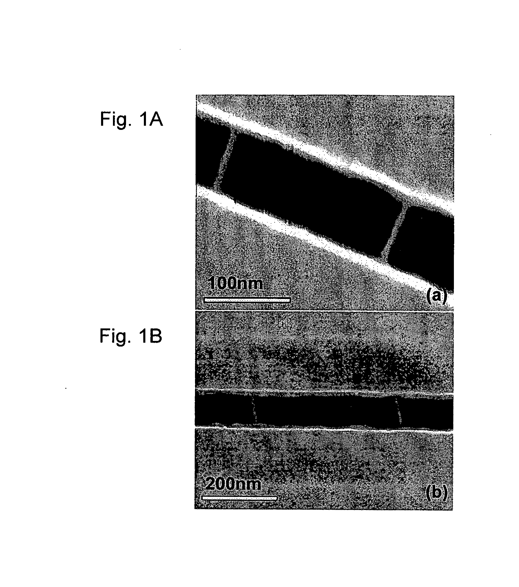
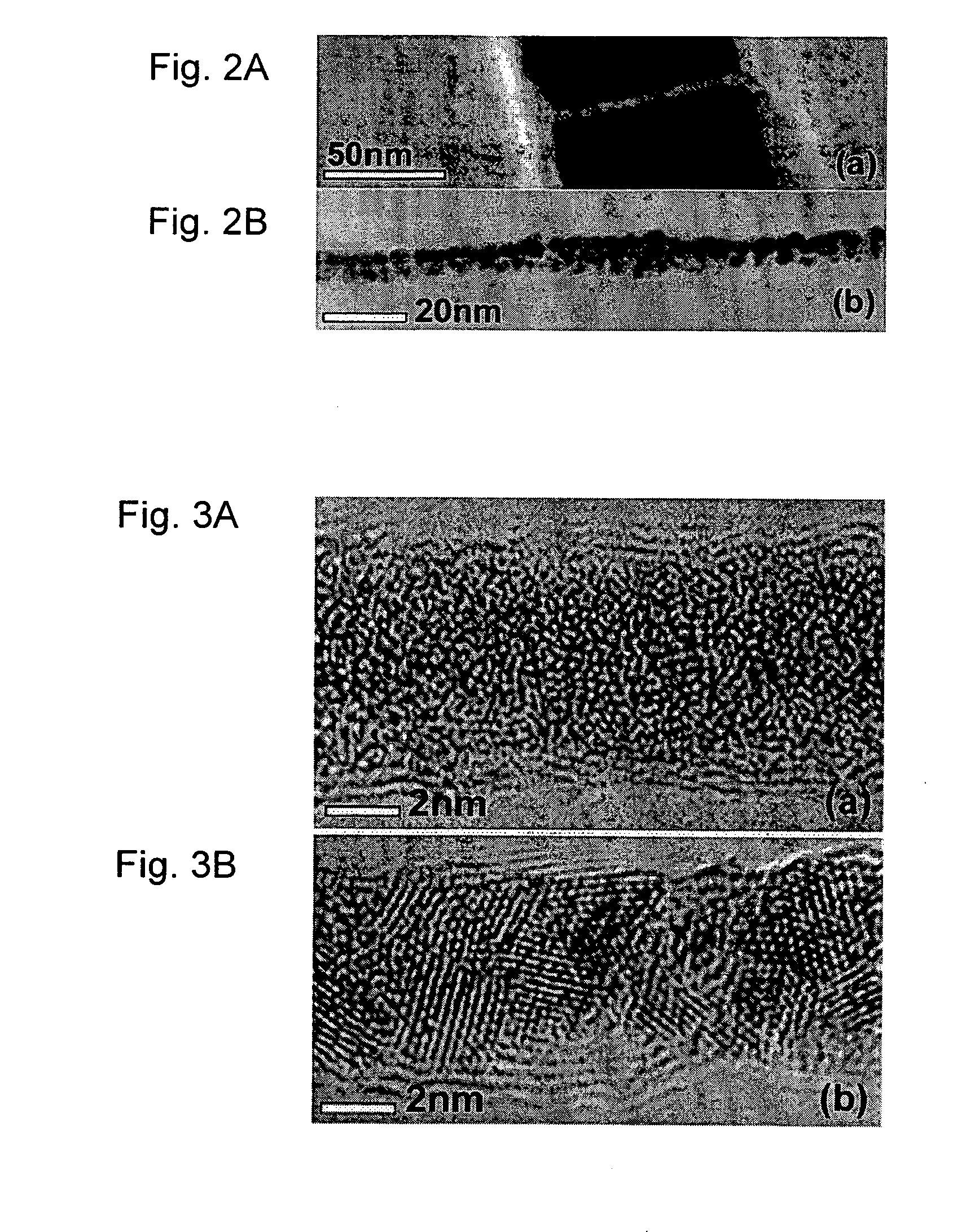
Processing methods of the present invention are capable of providing local modification of the shape of selected regions of a nanowire with a resolution equal to about 3 nanometers.
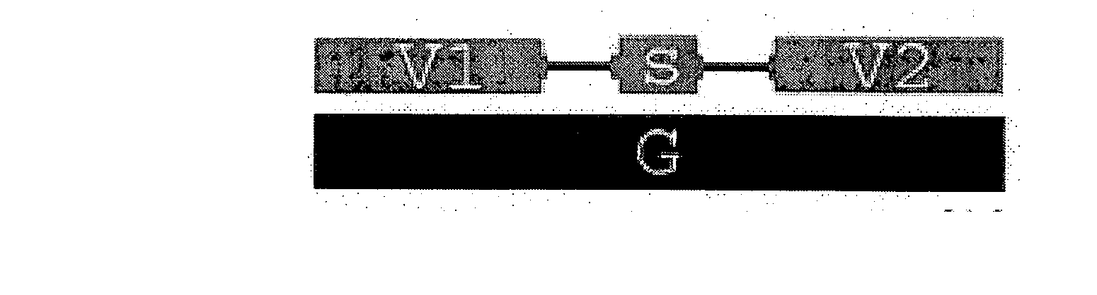
[0012] First conductance constricting segments, second conductance constricting segments and / or the middle conductive segments of this aspect of the present invention may have electrical properties, such as conductances, electrical resistances and capacitances, selected for a given application, such as use in a nanoelectrical or nanoelectromechanical device. For example, in one useful embodiment the first conductance constricting segment, second conductance constricting segment or both have a resistance equal to or greater than about 12 kΩ, and preferably for some applications equal to or greater than about 25 kΩ. Alternatively, first conductance constricting segment, second conductance constricting segment or both may comprise thin insulating nanowire segments, such as
metal oxide segments.
High resistance and / or insulating conductance constricting segments are useful for limiting the propagation of electrons in a manner localizing the electronic wave functions of electrons in the middle conductive segment, for example to generate a middle conductive segment comprising a Coulomb island. In one embodiment, for example, the presence of first and second
high resistance and / or insulating conduction constricting segments prevents mixing of the
electronic states of electrons on the middle conductive segment with external states, thereby providing
electron confinement in a Coloumb island of a SET
transistor. The present invention also provides nanowire configurations having a middle conductive element with a
capacitance low enough to provide a charging energy that is greater, for example a factor of 10 times greater, than thermal electronic fluctuations at a selected temperature, such a
capacitance low enough to provide a charging energy that is less than thermal electronic fluctuations at
room temperature (298 K).
[0014] In an embodiment, conductance constricting segments of the present invention have average cross sectional dimensions equal to about 6 nanometers or less, and preferably for some applications equal to about 3 nanometers or less. In an embodiment, conductance constricting segments of the present invention extend along the length of the nanowire distances equal to a value selected over the range of about 1 nanometer to about 100 nanometers. Selection of the cross sectional dimension and length provides conductance constricting segments having an accurately selected electrical resistance, including
high resistance conductance constricting segments. Selection of narrow cross sectional dimensions, for example cross sectional dimensions less than about 5 nanometers, allows fabrication of insulating conductance constricting segments via oxidation initiated by
exposure of narrow conductance constricting segments to an oxidizing medium such as
oxygen.
[0015] In an embodiment, the middle conductive segment has an average cross sectional dimension equal to or less than about 10 nanometers, more preferably for some applications equal to or less than about 6 nanometers. In an embodiment, the middle conductive segment extends along the length of the nanowire a distance equal to or less than about 20 nanometers, more preferably for some applications equal to or less than about 10 nanometers. Selection of small cross sectional dimensions, for example cross sectional dimensions less than about 6 nanometers, and short lengths, for example lengths less than about 10 nanometers, achieves capacitances and charging energies providing middle conductive segments useful as Coulomb islands in SET transistors.
[0017] In one embodiment, the positions of conductance constricting segments and conductive segments along the length of the nanowire are selected with great placement accuracy. For example, selection of the positions of first and second position of conductance constricting segments along the length of a nanowire to within about 10 nanometers or less provides a means of selecting the length of the middle conductive segment with good accuracy

