

Plasma processing apparatus
- Summary
- Abstract
- Description
- Claims
- Application Information
AI Technical Summary
Benefits of technology
Problems solved by technology
Method used
Image

Examples
embodiment 1
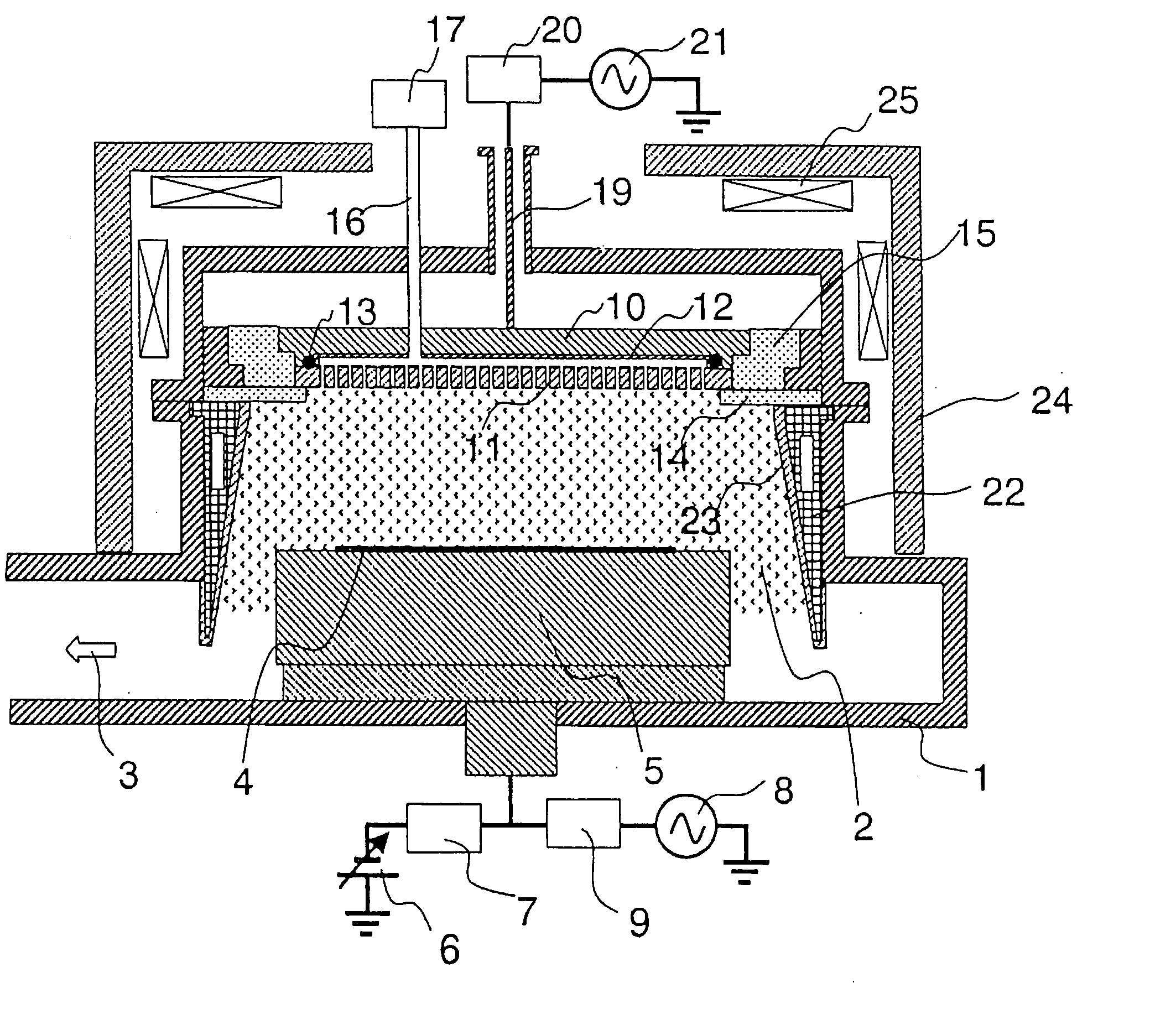
[0041] The first preferred embodiment of the present invention will be described with reference to a schematic view of the plasma processing apparatus illustrated in FIG. 1. A substrate 4 to be processed such as a semiconductor wafer or a liquid crystal device substrate is placed on a substrate holding electrode 5 having a function of an electrostatic chuck to which high frequency power can be applied. The substrate holding electrode 5 is equipped with a high-frequency power supply 8 with a frequency of 10 MHz or smaller, a matching circuit 9, and a DC power supply 6 and a filter circuit 7 for realizing electrostatic chuck. The processing chamber 1 is evacuated 3 via an exhaust system not shown, by which the pressure within the processing chamber 1 is controlled to a predetermined pressure. The high-frequency power for generating plasma 2 is supplied from a high-frequency power supply 21 having a frequency of 100 MHz to 500 MHz via an automatic matching box 20 through a coaxial line...
embodiment 2
[0058] The second embodiment of the present invention will now be described with reference to the schematic view of a plasma processing apparatus of FIG. 6. According to the present embodiment, high-frequency power for generating plasma is supplied to a high-frequency electrode 33 via a coaxial line 42. The high-frequency electrode 33 is disposed in the processing chamber via an insulating member 36 made of quartz and O-rings 35 which maintain the chamber in a vacuum state. The process gas used for processing is supplied through gas discharge holes 32 on a gas shower plate 31 formed of quartz disposed on a front side of the high-frequency electrode 33 to plasma. The process gas is supplied via a gas supply pipe 37 to the space formed at the side wall of the gas shower plate 31. Y2O3 ceramic is sprayed onto the surface of the space formed at the side wall of the gas shower plate 31 and on the surface of the high-frequency electrode 33 exposed to high-pressure process gas to form coat...
embodiment 3
[0061] The third embodiment of the present invention will be described with reference to the schematic view of the plasma processing apparatus of FIG. 7. According to the present embodiment, high-frequency radiation used for generating plasma is supplied to a high-frequency electrode 53 via a coaxial line 62. The high-frequency electrode 53 is disposed in the processing chamber via an insulating member 56 made of quartz and O-rings 55 which maintain the chamber in a vacuum state. A protecting plate 58 formed of a quartz panel or a polymer sheet is attached to the surface of the high-frequency electrode 53 and the surface of the conductor constituting the processing chamber. The process gas used for processing is supplied through gas discharge holes 52 on a gas shower plate 51 formed of quartz disposed on a front side of the high-frequency electrode 53 toward plasma. The process gas is supplied via a gas supply pipe 57 to the space formed at the side wall of the gas shower plate 51. ...
PUM
| Property | Measurement | Unit |
|---|---|---|
| Thickness | aaaaa | aaaaa |
| Thickness | aaaaa | aaaaa |
| Thickness | aaaaa | aaaaa |
Abstract
Description
Claims
Application Information