Low cost InGaAIN based lasers

a laser and low-cost technology, applied in semiconductor lasers, optical head manufacturing, optical beam sources, etc., to achieve the effect of minimizing the obstruction of laser light, high intensity, and high optical wavefront quality

Active Publication Date: 2007-03-01
MACOM TECH SOLUTIONS HLDG INC
View PDF8 Cites 25 Cited by
  • Summary
  • Abstract
  • Description
  • Claims
  • Application Information

AI Technical Summary

Benefits of technology

[0026] According to the present invention, the distance a between the edge of the chip and the bottom of the laser mesa and the height h between the center of the laser output beam and the top of the laser mesa must be chosen with particular attention to the beam divergence of the laser radiation emitted from the front laser mirror. In the direction perpendicular to the substrate, the radiation emerging from the front laser mirror has high intensity in the beam center and falls off over an extended distance away from the beam center. The vertical divergence of the emitted laser beam is typically characterized by its full-width-half-maximum farfield angle marking the angular

Problems solved by technology

However, the need for special choices of laser waveguide length and width to minimize yield reductions caused by material defects has not bee

Method used


Image

  • Low cost InGaAIN based lasers
  • Low cost InGaAIN based lasers
  • Low cost InGaAIN based lasers

Examples


Embodiment Construction

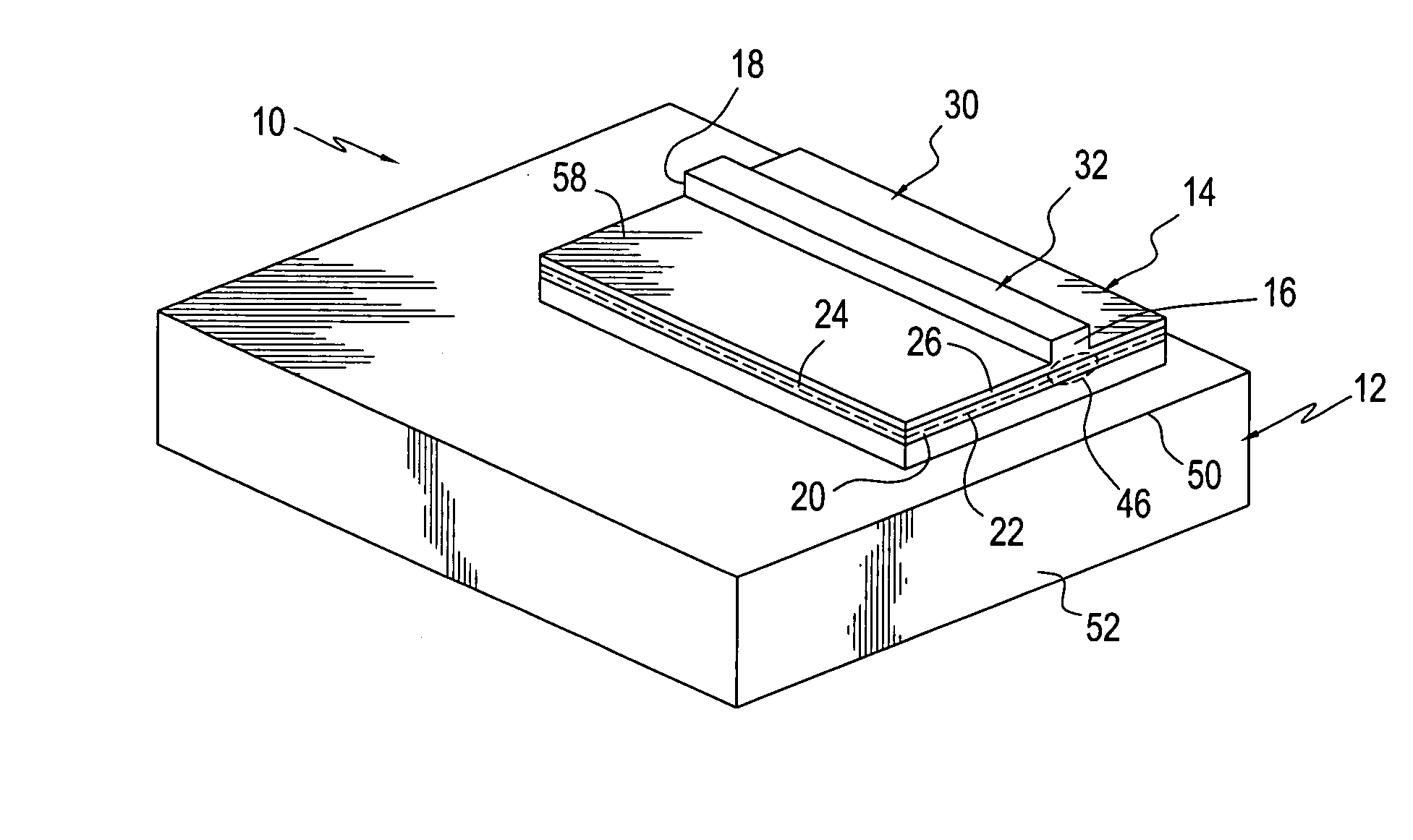
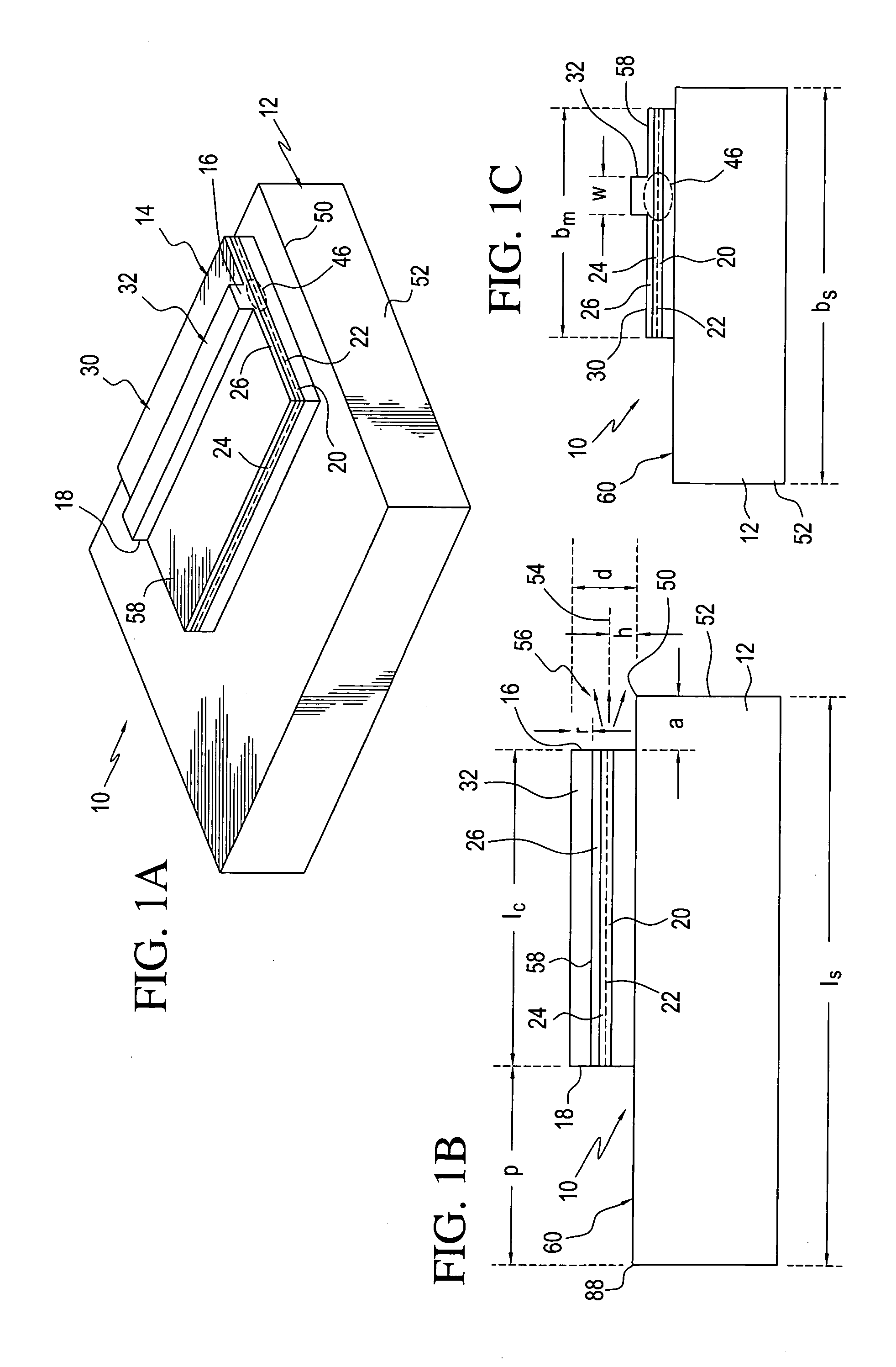
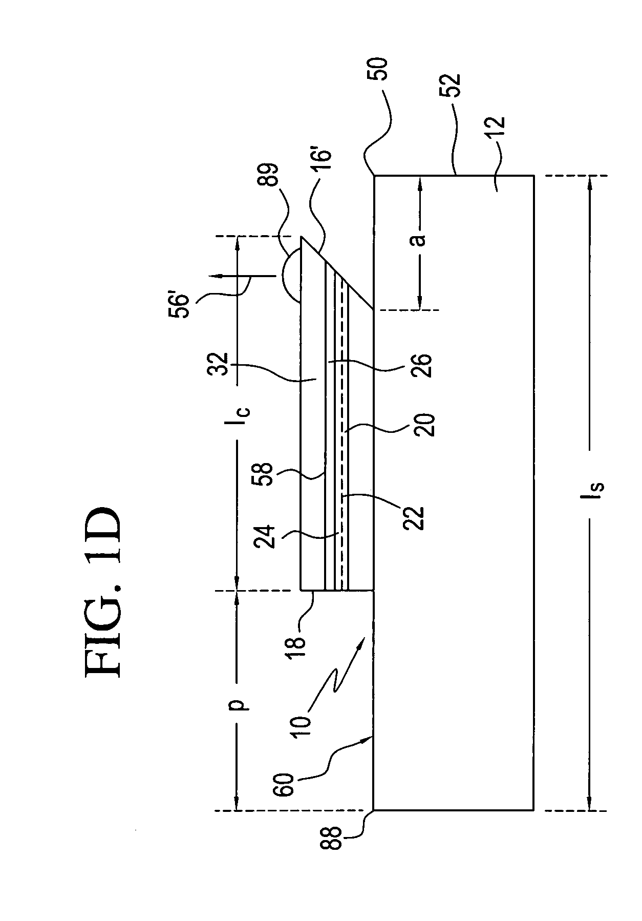
[0041] Turning now to a detailed description of the invention, FIGS. 1A-1C illustrate a diode laser chip 10, including a substrate 12 supporting an epitaxially grown and etched ridge laser 14 having end facets 16 and 18. The ridge laser is formed by etching of the laser end facets, as is known in the art, with the present laser having a special design geometry. In accordance with the invention, the semiconductor laser structure 14 is epitaxially grown on substrate 12 with at least a lower cladding layer 20, an active layer 22, an upper cladding layer 24, and a contact layer 26. Dry etching through a lithographically defined mask produces a laser mesa 30 of length lc and width bm. Another sequence of lithography and etching is used to form the ridge structure 32 with width w on top of the mesa. While the laser schematically shown in FIGS. 1A-C and described above is a ridge-type design, it is understood that this invention is not limited to ridge laser structures and also applies to ...


PUM


Abstract

A method and structure for producing lasers having good optical wavefront characteristics, such as are needed for optical storage includes providing a laser wherein an output beam emerging from the laser front facet is essentially unobstructed by the edges of the semiconductor chip in order to prevent detrimental beam distortions. The semiconductor laser structure is epitaxially grown on a substrate with at least a lower cladding layer, an active layer, an upper cladding layer, and a contact layer. Dry etching through a lithographically defined mask produces a laser mesa of length lc and width bm. Another sequence of lithography and etching is used to form a ridge structure with width w on top of the mesa. The etching step also forming mirrors, or facets, on the ends of the laser waveguide structures. The length ls and width bs of the chip can be selected as convenient values equal to or longer than the waveguide length lc and mesa width bm, respectively. The waveguide length and width are selected so that for a given defect density D, the yield YD is larger than 50%.

Description

[0001] This application claims the benefit of U.S. Provisional Application No. 60 / 710,882, filed Aug. 25, 2005, the disclosure of which is hereby incorporated herein by reference.FIELD OF THE INVENTION [0002] The present invention relates to semiconductor diode lasers and, more specifically, to low-cost InGaAlN based lasers with etched facets. BACKGROUND OF THE INVENTION [0003] InGaAlN diode lasers are of interest as light sources for a number of applications; for example, in high-density optical storage, displays, printing and biomedicine. In many devices and systems associated with these applications, laser sources are needed that are capable of providing an output beam with high wavefront quality. Furthermore, the widespread use and commercial success of many of these systems and devices depend on the ability to provide them at low cost. Consequently, high manufacturing yields and low cost are critical requirements for the light sources needed to construct such systems and device...

Claims


Application Information

Patent Timeline
IPC IPC(8): H01L33/00G11B7/125H01S5/185
CPCG11B7/127G11B7/22H01S5/0201H01S5/0207H01S5/026H01S2301/18H01S5/18H01S5/22H01S5/32341H01S5/4056H01S5/1039H01S5/0042H01S5/185
Inventor BEHFAR, ALEX A.LENTH, WILFRIED
Owner MACOM TECH SOLUTIONS HLDG INC
Why Eureka
Try Eureka