

Etch masks based on template-assembled nanoclusters
- Summary
- Abstract
- Description
- Claims
- Application Information
AI Technical Summary
Benefits of technology
Problems solved by technology
Method used
Image

Examples
examples
[0229] The invention is further illustrated by the following examples:
1. Lithography Processes
[0230] Combinations of optical and Electron Beam Lithography and their use in the formation of surface features and contacts have been described in a previous patent application [9] and are hereby incorporated by reference.
2. Results of Cluster Deposition Experiments
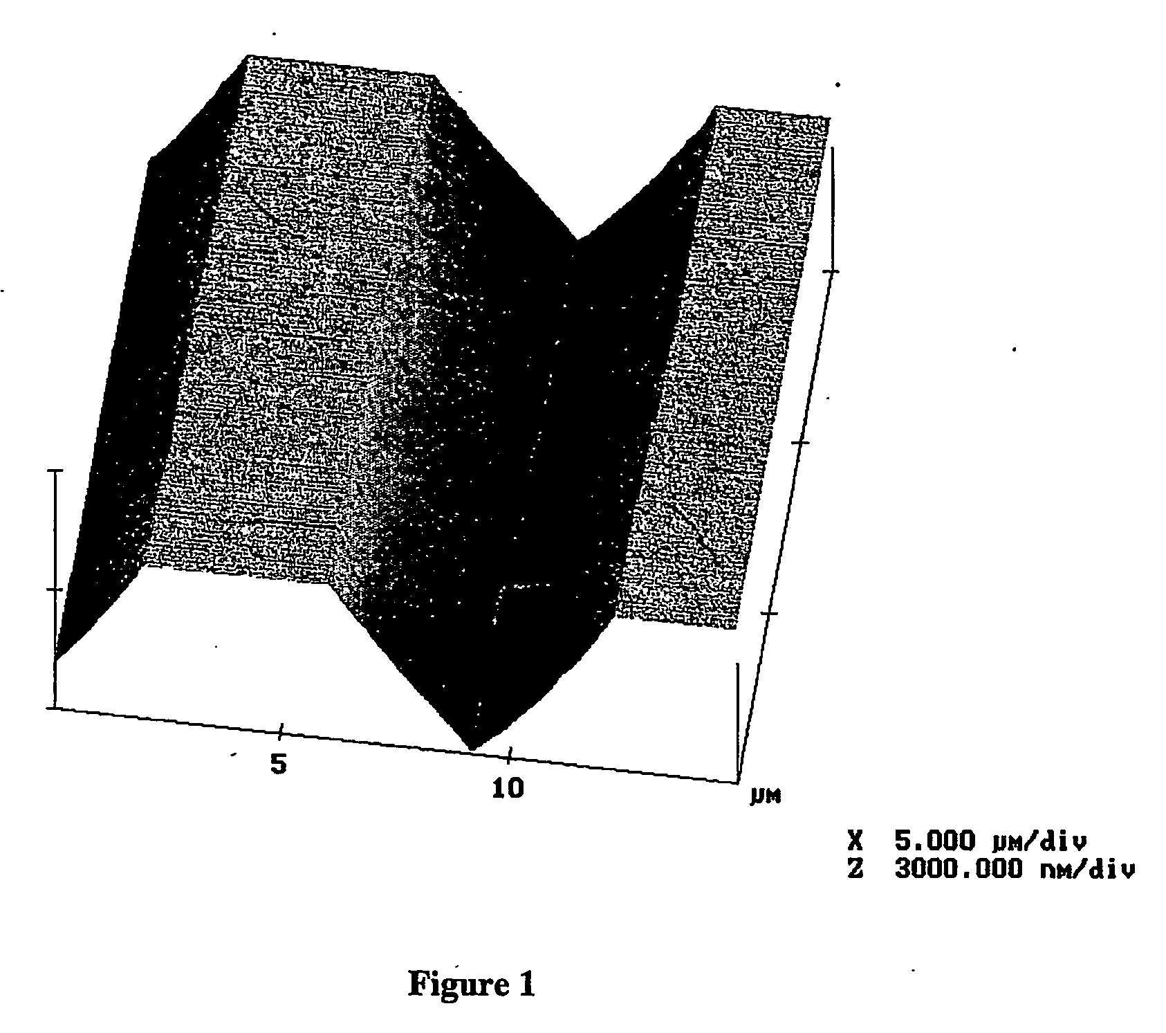
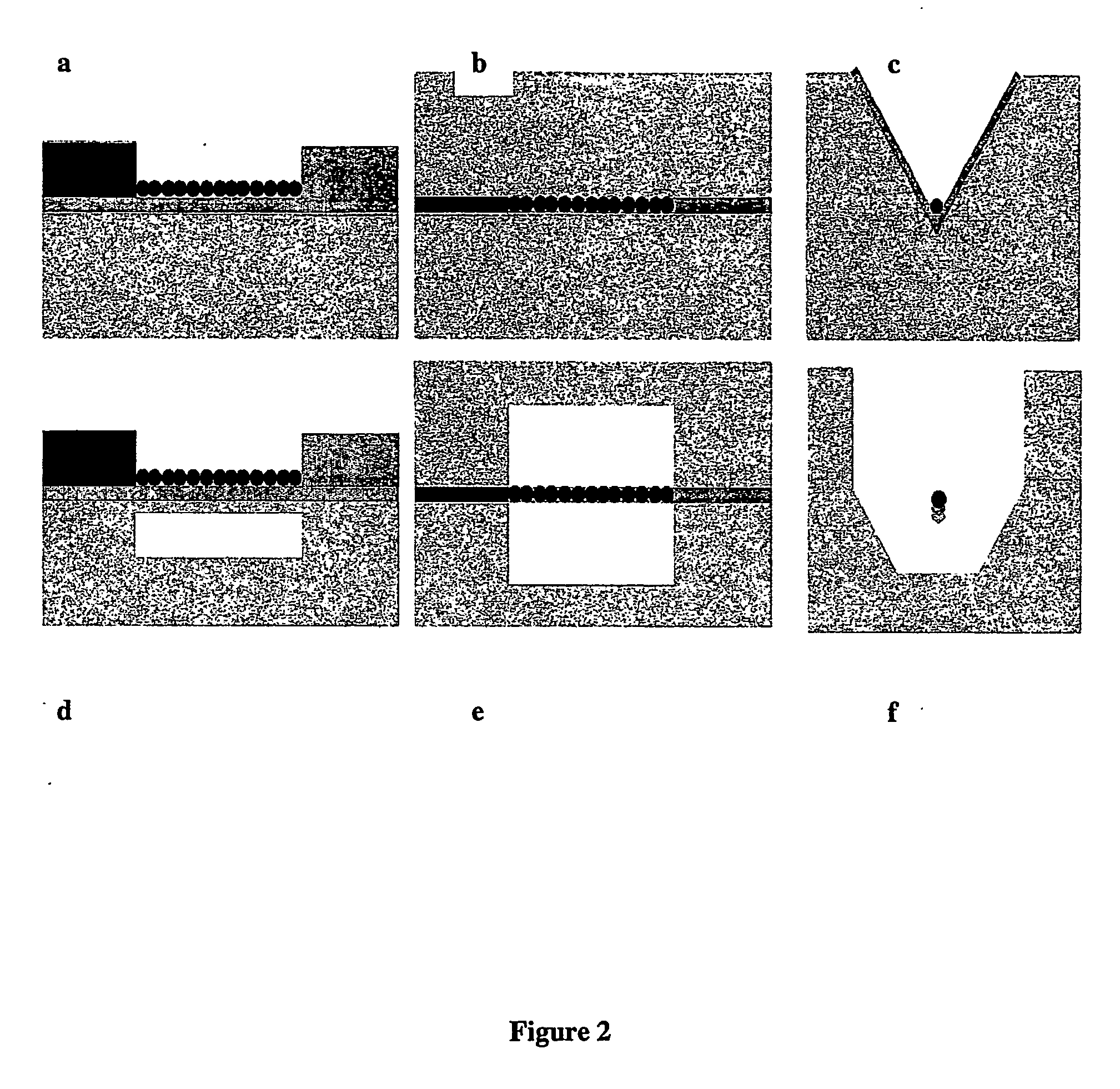
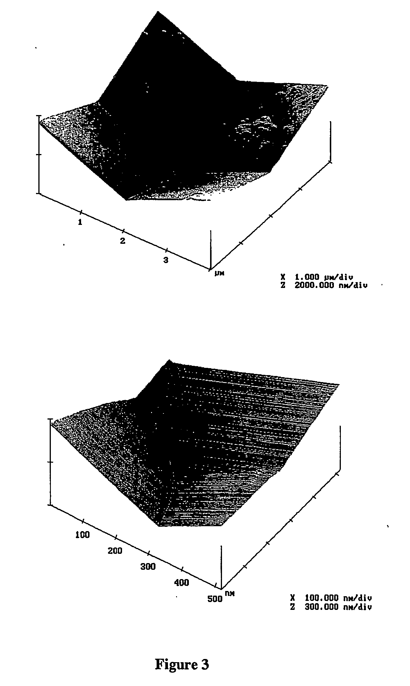
[0231] Deposition of bismuth clusters onto plain SiN surfaces (or such surfaces with predefined electrical contacts) and the imaging of such cluster films using atomic force, optical and field emission scanning electron microscopy (FE-SEM) has been described in a previous patent application [9] and are hereby incorporated by reference. The FE-SEM images in that previous work show that the clusters do not diffuse and coalesce significantly on SiN: there is a limited amount of coalescence—the clusters merge very slightly into their neighbours—but in general the particles are still distinguishable. On V-grooves (see images in F...
PUM
 Abstract
Description
Claims
Application Information