Quantum dot light emitting layer

Inactive Publication Date: 2007-03-15
NANOCO TECH LTD
View PDF4 Cites 297 Cited by
  • Summary
  • Abstract
  • Description
  • Claims
  • Application Information

AI Technical Summary

Benefits of technology

[0012] It is an advantage of the present invention to provide a way of forming a light emitting layer, whose emitting species are quantum dots, that is simultaneously luminescent and conductive. The light emitting layer includes a composite of conductive wide band gap nanoparticles and shelled quantum dot emitters. A thermal anneal is used to sinter the conductive nanoparticles amongst themselves and onto the surface of the quantum dots. As a result, the conductivity of the light emitting layer is enhanced, as is electron-hole injection into the quantum dots. To enable the quantum dots to survive the anneal step without a loss in their fluorescent efficiency (since the organic ligands passivating the quantum dots boil away during the anneal process), the quantum dot shells are engineered to confine the electrons and holes, such that, their wavefunctions do not sample the surface states of the outer s

Problems solved by technology

The dominant ones are high manufacturing costs, difficulty in combining multi-color output from the same chip, the need for high cost and rigid substrates.
In comparison to crystalline-based inorganic LEDs, OLEDs have much reduced brightness (mainly due to small carrier mobilities), shorter lifetimes, and require expensive encapsulation for device operation.
Because of problems, such as, aggregation of the quantum dots in the emitter layer, the efficiency of these devices was rather low in comparison with typical OLED devices.
The efficiency was even poorer when a neat film of quantum dots was used as the emitter layer (Hikmet et al., J. Appl

Method used


Image

  • Quantum dot light emitting layer
  • Quantum dot light emitting layer
  • Quantum dot light emitting layer

Examples


example 1

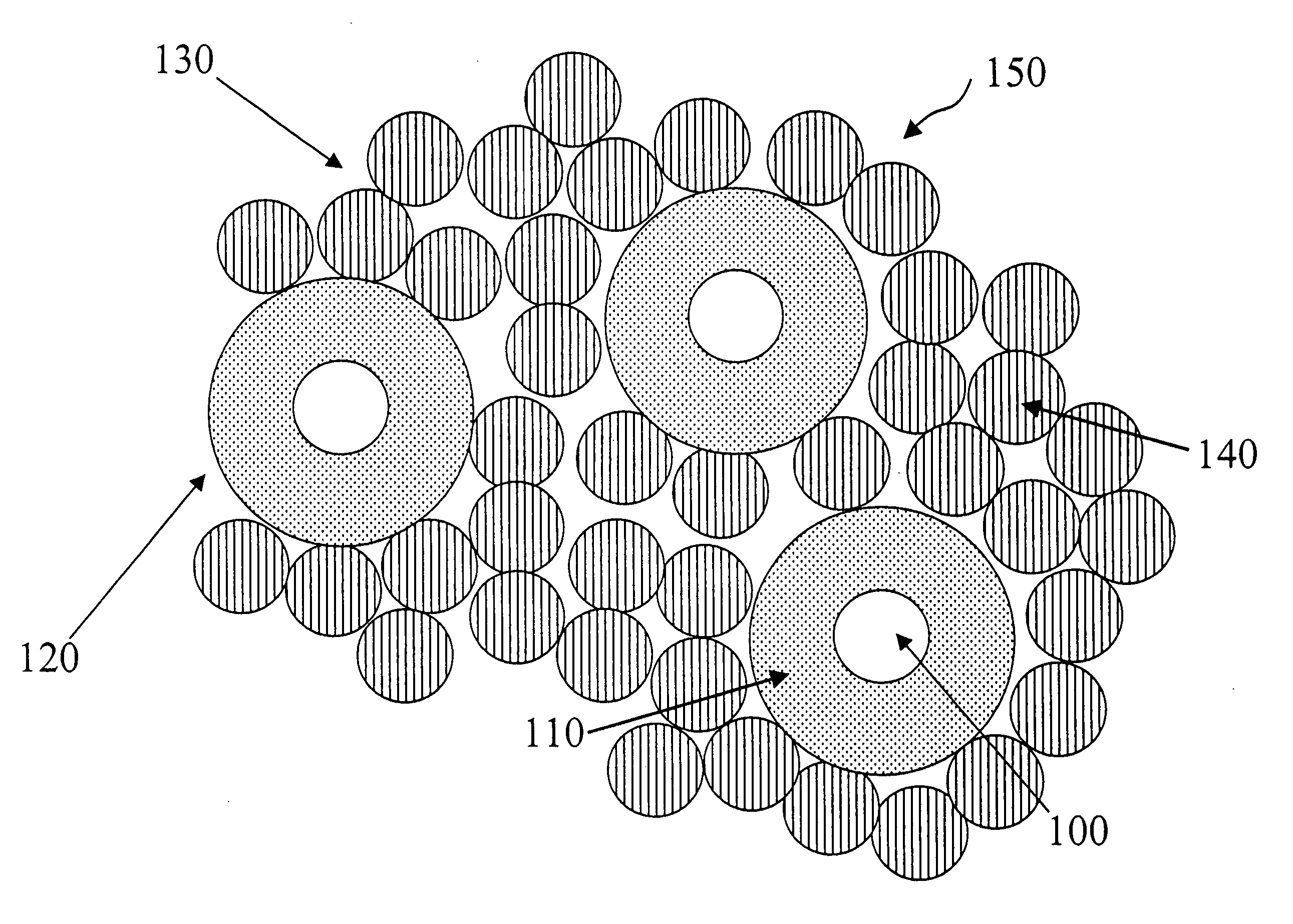
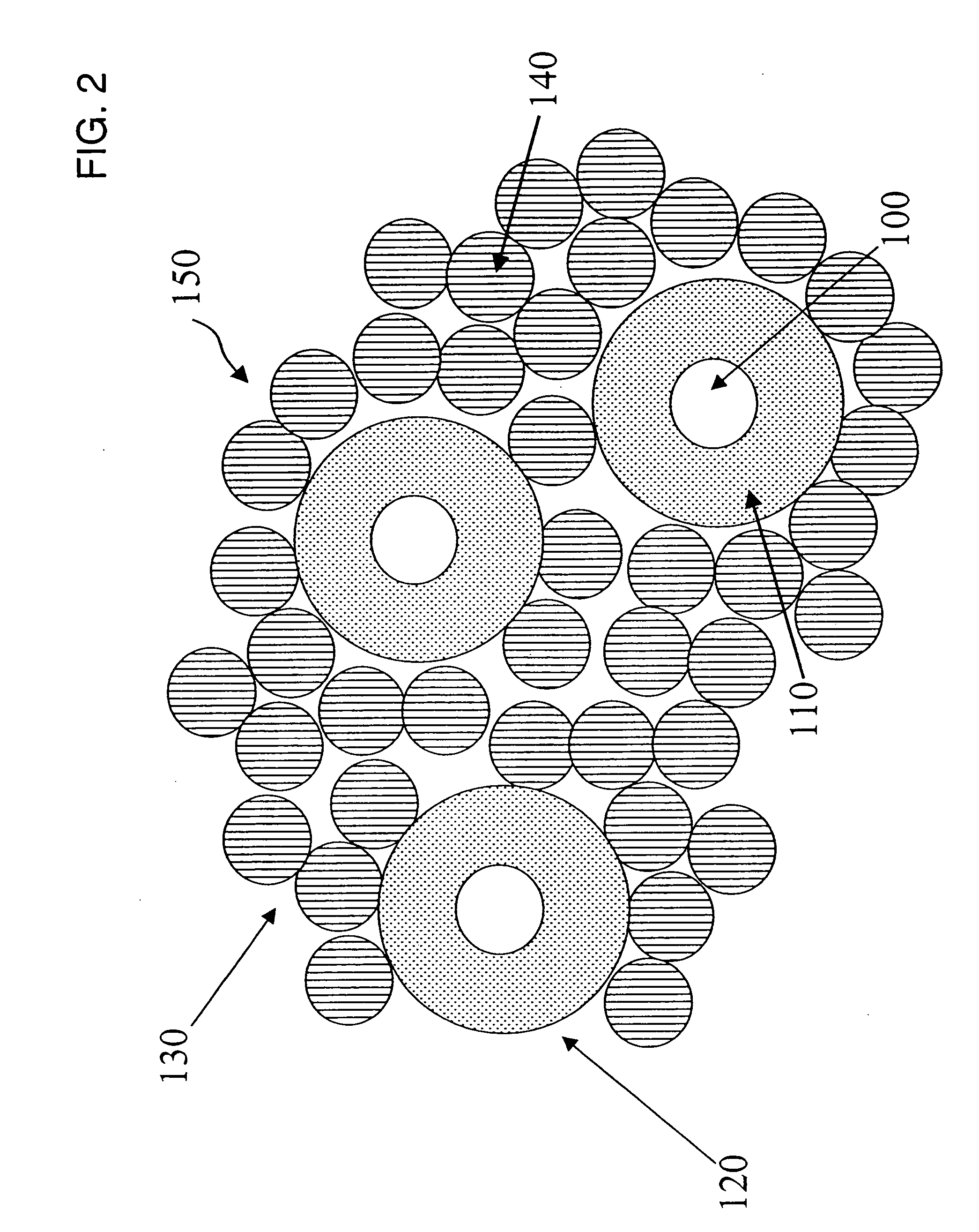
[0031] An inorganic light emitting layer 150 was formed in accordance with the schematic of FIG. 2. The inorganic nanoparticles 140 were composed of ZnS, while the core / shell quantum dots 120 had a CdSe core and a ZnSe / ZnS shell. The ZnS particles were chemically synthesized using an adaptation of the method reported by Khosravi et al. (A. A. Khosravi et al., Appl. Phys. Lett. 67, 2506 [1995]). The Zn source was ZnCl2, the sulfur source was bis(trimethlysilyl)sulfide (TMS)2S, and the surfactant / ligand was hexylamine. Butanol solutions of ZnCl2, (TMS)2S, and hexylamine, each at 0.02 M, were prepared and equal volume of each solution was used in the reaction. To prevent the oxidation of the resulting ZnS nanoparticles, the reaction was performed under inert conditions using well-known procedures. Initially, 5 ml of the zinc chloride solution and 5 ml of the hexylamine solution are combined in a two-neck flask, while vigorously stirring the mixture. Next, 5 ml of the (TMS)2S solution i...

example 2

[0035] Electroluminescent light emitting diodes were constructed using the above inorganic light emitting layer 120 as a component. ITO was sputtered onto the surface of a cleaned glass substrate 160 through a shadowmask. Following the deposition, the ITO film was annealed at 300° C. for 1 hour to improve its transparency. Next the inorganic light emitting layer 120, as described in Example 1, was deposited on the surface of the ITO. To ensure a pinhole free layer, the composite (ZnS nanoparticles and CdSe / ZnSe / ZnS core / shell / shells) colloidal dispersion was drop cast twice (each drop cast was followed by a 50 minute anneal at 270° C. in the tube furnace). Prior to the two drop casts, the deposition surface was cleaned by an acetone / methanol solvent wash, followed by blow drying the sample with nitrogen.

[0036] Next the n-type transport layer 230 was deposited. It was formed from ZnSe nanoparticles. The nanoparticles were synthesized (carried out under Schlenk line and argon flow) u...


PUM


Abstract

An inorganic light emitting layer having a plurality of light emitting cores, each core having a semiconductor material that emits light in response to recombination of holes and electrons, each such light emitting core defining a first bandgap; a plurality of semiconductor shells formed respectively about the light emitting cores to form core/shell quantum dots, each such semiconductor shell having a second bandgap wider than the first bandgap; and a semiconductor matrix connected to the semiconductor shells to provide a conductive path through the semiconductor matrix and to each such semiconductor shell and its corresponding light emitting core so as to permit the recombination of holes and electrons.

Description

FIELD OF THE INVENTION [0001] The present invention relates to an inorganic light emitting diode device that includes a light emitting layer having quantum dots. BACKGROUND OF THE INVENTION [0002] Semiconductor light emitting diode (LED) devices have been made since the early 1960's and currently are manufactured for usage in a wide range of consumer and commercial applications. The layers comprising the LEDs are based on crystalline semiconductor materials which require ultra-high vacuum techniques for their growth, such as, molecular organic chemical vapor deposition. In addition, the layers typically need to be grown on nearly lattice-matched substrates in order to form defect-free layers. These crystalline-based inorganic LEDs have the advantages of high brightness (due to layers with high conductivities), long lifetimes, good environmental stability, and good external quantum efficiencies. The usage of crystalline semiconductor layers that results in all of these advantages, al...

Claims


Application Information

Patent Timeline
IPC IPC(8): H01L33/00H01L33/08
CPCB82Y10/00B82Y20/00B82Y30/00H05B33/14C09K11/565C09K11/883H01L33/08C09K11/02Y10S977/95C09K11/08
Inventor KAHEN, KEITH B.
Owner NANOCO TECH LTD
Why Eureka
Try Eureka