Electroluminescent device

a technology of electroluminescent devices and light-emitting diodes, which is applied in the direction of discharge tube luminescnet screens, other domestic articles, natural mineral layered products, etc., can solve the problems of large loss of efficiency, and insufficient triplet energies of common host materials, such as cbp, to achieve efficient hosts. , good luminance and reduced drive voltage

Active Publication Date: 2007-04-19
GLOBAL OLED TECH
View PDF10 Cites 406 Cited by
  • Summary
  • Abstract
  • Description
  • Claims
  • Application Information

AI Technical Summary

Benefits of technology

[0012] The light-emitting layer emits blue light and provides good luminance and reduced drive voltage.

Problems solved by technology

While organic electroluminescent (EL) devices have been known for over two decades, their performance limitations have represented a barrier to many desirable applications.
However, it is generally believed that only 25% of the excitons created in an EL device are singlet excitons.
This results in a large loss in efficiency since 75% of the excitons are not used in the light emission process.
In the case of phosphorescent materials that emit blue light, most common host materials, such as CBP, do not have high enough triplet energies to act as efficient hosts.
Many of these materials do not have charge-carrying abilities and in some cases, when incorporated in an OLED device, they can result in high drive voltages.

Method used


Image

  • Electroluminescent device
  • Electroluminescent device
  • Electroluminescent device

Examples


example 1

[0236] Synthesis of Inv-1.

[0237] Inv-1 was prepared by the following procedure (eq. 1 and eq. 2). A solution of 1,4-dibromobenzene (2.359 g, 10mmol) in ether (55 ml) was stirred at −40° C. under dry N2 and treated with a solution of butyllithium (2.5 M in hexane, 10 mmol). The resulting mixture was kept at −10° C. for 15 min, and then SiPh2Cl2 (0.93 ml, 4.5 mmol) was added quickly. The mixture was stirred at −10° C. for 30 min and at room temperature overnight. Then water was added, and the mixture was extracted with a combination of ether and dichloromethane. The combined extracts were washed with water, dried over MgSO4, and filtered. Volatiles were removed by evaporation under reduced pressure, and the residue was purified by column chromatography on silica gel with 7% toluene / hexane. This afforded bis(4-bromophenyl)diphenylsilane (Int-1) in 75% yield.

[0238] Bis(4-bromophenyl)diphenylsilane (3.2 g, 6.5 mmol) was dissolved in 40 ml dry THF. The solution was cooled to −78° C., a...

example 2

[0239] Synthesis of Inv-10.

[0240] Inv-10 was prepared by the following procedure (eq. 3 and eq. 4). A solution of 4-fluorobromobenzene (4.2 g, 24 mmol) in ether (55 ml) was stirred at −40° C. under dry N2 and treated with a solution of butyllithium (1.6 M in hexane, 20 mmol). The resulting mixture was kept at −40° C. for 30 min, and then SiPh2Cl2 (1.85 ml, 9 mmol) was added quickly. The mixture was stirred at −40° C. for 30 min and then at room temperature overnight. Volatiles were removed by evaporation under reduced pressure, and the residue was recrystallized from ether / methanol twice to give bis(4-difluorophenyl)diphenylsilane (Int-2) as colorless crystals; yield: 62%.

[0241] Sodium hydride (0.44 g, 11 mmol, in the form of a 60 wt % suspension in mineral oil) was added to a stirred solution of diphenylphosphineoxide (2.22 g, 11 mmol) in dry N,N′-dimethylformamide (40 ml) at room temperature under nitrogen. With evolution of hydrogen a yellow solution was formed. Then, bis(4-di...

example 3

Fabrication of EL Devices 1-1, 1-2, and 1-3.

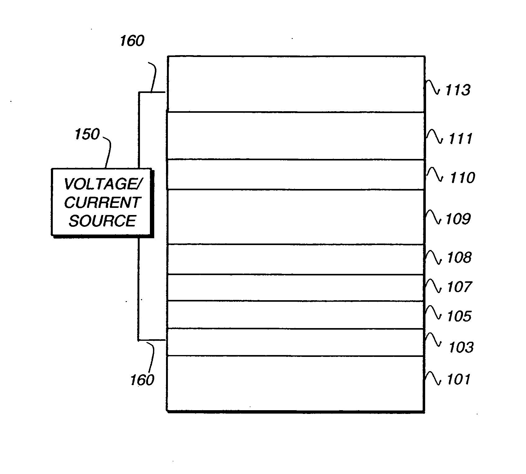
[0242] EL device 1 -1, satisfying the requirements of the invention, was constructed in the following manner.

[0243] A glass substrate coated with an 21.5 nm layer of indium-tin oxide (ITO) as the anode was sequentially ultrasonicated in a commercial detergent, rinsed in deionized water, degreased in toluene vapor and exposed to oxygen plasma for about 1 min. [0244] a) Over the ITO was deposited a 1 nm fluorocarbon (CFx) hole-injecting layer (HIL) by plasma-assisted deposition of CHF3. [0245] b) A hole-transporting layer (HTL-1) of N,N′-di-1-naphthalenyl-N,N′-diphenyl-4,4′-diaminobiphenyl (NPB) having a thickness of 75 nm was then evaporated onto a). [0246] c) An exciton-blocking layer (EBL) of 4,4′,4″-tris(N-carbazolyl) triphenylamine (TCTA) having a thickness of 10 nm was then deposited. [0247] d) A 35 nm light-emitting layer (LEL) including a primary host, Inv-1; and 8% by volume of a phosphorescent light emitting material, D-1, was t...


PUM

PropertyMeasurementUnit
LUMO energyaaaaaaaaaa
ionization potentialaaaaaaaaaa

Abstract

An OLED device comprises a cathode and an anode and has located therebetween a light-emitting layer comprising a phosphorescent light-emitting material and a host comprising a compound of a tetravalent atom wherein the four groups bonded to the atom are aromatic rings, at least one of which contains an electron-withdrawing group (EWG) substituent comprising at least three atoms, the compound having a triplet energy of at least 2.7 eV and a LUMO energy within 0.6 eV of the LUMO energy of at least one material in an adjacent layer on the cathode side of the light-emitting layer. Particular embodiments include certain tetravalent silicon compounds. The light-emitting layer emits blue light and provides good luminance and reduced drive voltage.

Description

FIELD OF THE INVENTION [0001] This invention relates to an organic light emitting diode (OLED) electroluminescent (EL) device comprising a light-emitting layer containing a phosphorescent light-emitting material and a host material that can provide desirable electroluminescent properties. BACKGROUND OF THE INVENTION [0002] While organic electroluminescent (EL) devices have been known for over two decades, their performance limitations have represented a barrier to many desirable applications. In simplest form, an organic EL device is comprised of an anode for hole injection, a cathode for electron injection, and an organic medium sandwiched between these electrodes to support charge recombination that yields emission of light. These devices are also commonly referred to as organic light-emitting diodes, or OLEDs. Representative of earlier organic EL devices are Gurnee et al. U.S. Pat. No. 3,172,862, issued Mar. 9, 1965; Gurnee U.S. Pat. No. 3,173,050, issued Mar. 9, 1965; Dresner, “...

Claims


Application Information

Patent Timeline
Patent Type & Authority Applications(United States)
IPC IPC(8): H01L51/54
CPCC09K11/06C09K2211/1007C09K2211/1011C09K2211/1014C09K2211/1033C09K2211/1037C09K2211/1044C09K2211/1055C09K2211/107C09K2211/1088C09K2211/185H01L51/008H01L51/0085H01L51/0094H01L51/5016H05B33/20Y10S428/917H10K85/322H10K85/342H10K85/40H10K50/11H10K2101/10
Inventor REN, XIAOFANBROWN, CHRISTOPHER T.
Owner GLOBAL OLED TECH
Why Eureka
Try Eureka