Liquid crystal display device and dielectric film usable in the liquid crystal display device

a technology of liquid crystal display device and dielectric film, which is applied in the direction of thin material processing, instruments, chemistry apparatus and processes, etc., can solve the problems of low number of processes required for deposition, difficulty in producing organic siloxane dielectric film with higher thickness, etc., and achieve high

Active Publication Date: 2007-04-26
PANASONIC LIQUID CRYSTAL DISPLAY CO LTD +1
View PDF1 Cites 61 Cited by
  • Summary
  • Abstract
  • Description
  • Claims
  • Application Information

AI Technical Summary

Benefits of technology

[0070] The dielectric film of the present invention exhibits high effects when it is applied as interlayer dielectric film of the liquid crystal display devi

Problems solved by technology

Moreover, the number of the processes required for the deposition is low.
However, the organic siloxane dielectric film has another problem, i.e. the difficulty to produce it with higher thickness.
When it is tried to increase the film thickness of the organic siloxane dielectric film, film stress is generated due to the film contraction caused by “siloxanization” of silanol, and cracking occurs on a portion where stress is concentrated.
In particular, in case there is a graded step in the underlying layer of the interlayer dielectric film, cracking is very likely to occur on or around the graded step.
Moisture absorption of the interlayer dielectric film due to cracking may decrease the reliability of TFT or and may cause lower reliability of the liquid crystal display device.
Thus, even when an interlayer dielectric

Method used


Image

  • Liquid crystal display device and dielectric film usable in the liquid crystal display device
  • Liquid crystal display device and dielectric film usable in the liquid crystal display device
  • Liquid crystal display device and dielectric film usable in the liquid crystal display device

Examples


example 1

[0087] Example 1 of the present invention relates to a method for forming a dielectric film suitable as an interlayer dielectric film of a liquid crystal display device and to a dielectric film obtained by the method. As the starting material for the dielectric film of Example 1, organic poly-silazane, which has a methyl group as an organic group and has a ratio of silicon content to carbon content (C content / Si content) being 1 in the element ratio is used, and a raw material solution, which contains a photo-acid generator diluted by propylene-glycol-monomethyl ether acetate (PGMEA) is used. This raw material solution was processed by spin coating at 500-3000 rpm on a silicon substrate or on glass substrate, and prebaking was performed using hot plate in nitrogen atmosphere at 90° C. for 90 seconds. The coated film thus obtained was processed by overall exposure, humidification, and thermal curing in this order under the condition shown in Table 1. For the overall exposure, a low p...

example 2

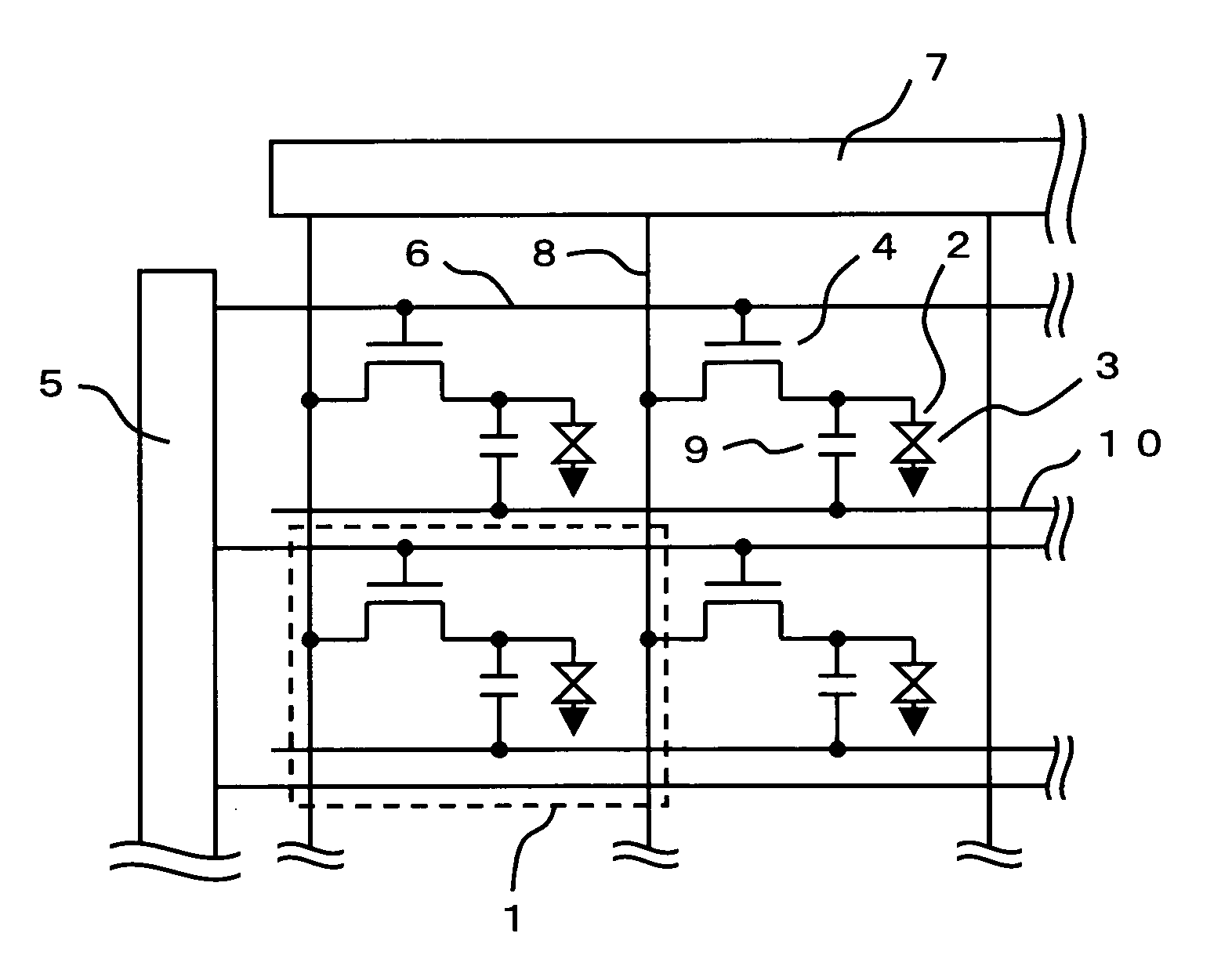
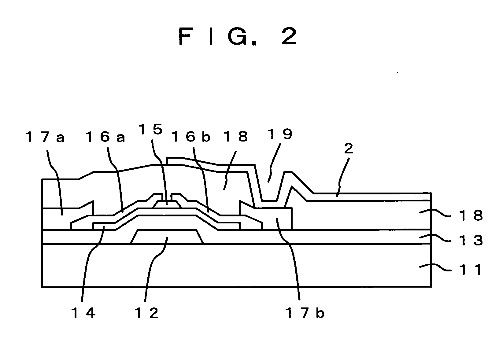
[0099] Example 2 relates to the liquid crystal display device of the present invention. In this Example 2, a process to form low temperature polysilicon TFT was taken as an example. FIG. 9 is a plan view of one pixel unit of TFT in the liquid crystal display device of the present invention. In the pixel, there are provided TFT comprising a polysilicon film 23a, a gate electrode 25a, a source wiring 28a, and a drain wiring 28b, and a capacity electrode 25b. Also, a pixel electrode 33a and the drain wiring 28b are superimposed on each other with the interlayer dielectric film interposed therebetween. FIG. 15 represents cross-sectional views, each showing TFT in the liquid crystal display device of the present invention along the line A-A′ in FIG. 9.

[0100]FIG. 10-FIG. 15 each represents drawings to explain a process for forming low temperature polysilicon TFT on the thin-film transistor substrate of the liquid crystal display device of active matrix mode. Description will be given bel...


PUM


Abstract

The present invention provides a liquid crystal display device with high image visibility at low power consumption and produced at low cost by using an interlayer dielectric film, which has low dielectric constant, high heat-resistant property, high optical transmissivity, high film thickness and high flattening property produced at low cost. An organic siloxane dielectric film is used as an interlayer dielectric film of the liquid crystal display device. A ratio of nitrogen content to silicon content (Ni content/Si content) in the interlayer dielectric film is controlled to 0.04 or more in the element ratio. The limiting film thickness to suppress and limit the cracking caused by the thickening of the interlayer dielectric film is set to 1.5 μm or more.

Description

BACKGROUND OF THE INVENTION [0001] 1. Field of the Invention [0002] The present invention relates to a liquid crystal display device of active matrix mode driven by thin-film transistor and to a dielectric film usable in the liquid crystal display device. [0003] 2. Description of the Prior Art [0004] Liquid crystal display device is widely used in applications as an image display device in various types of electronic devices such as thin-type television set, display for computer, portable terminal, etc. Most of the liquid crystal display devices are operated by a mode called active matrix mode. Specifically, there are provided thin-film transistor (TFT) to drive the liquid crystal for the pixels arranged in matrix form. As the types of TFT, amorphous silicon (a-Si; non-crystal silicon) TFT and polysilicon (poly-Si; polycrystal silicon) TFT are known. [0005] The amorphous silicon TFT can be formed on a substrate with larger area at low cost, and this has been widely used in the liqui...

Claims


Application Information

Patent Timeline
IPC IPC(8): C09K19/00
CPCG02F1/133345G02F1/1362G02F2202/02H01L21/02126Y10T428/10H01L21/02282H01L21/3122H01L21/31633H01L21/3185H01L21/02222C09K2323/00
Inventor RYUZAKI, DAISUKETORII, KAZUYOSHIHATANO, MUTSUKOSONODA, DAISUKEKANEKO, TOSHIKI
Owner PANASONIC LIQUID CRYSTAL DISPLAY CO LTD
Why Eureka
Try Eureka