Method for manufacturing semiconductor device, semiconductor device, and laser irradiation apparatus

a laser irradiation apparatus and semiconductor technology, applied in the direction of chemistry apparatus and processes, polycrystalline material growth, crystal growth process, etc., can solve the problem of rough surface of the semiconductor film, and achieve the effect of suppressing the variation of impurity concentration due to the fluctuation of energy density, suppressing the variation of on-current in addition to the mobility, and suppressing the variation of impurity concentration

Inactive Publication Date: 2007-05-03
SEMICON ENERGY LAB CO LTD
View PDF24 Cites 8 Cited by
  • Summary
  • Abstract
  • Description
  • Claims
  • Application Information

AI Technical Summary

Benefits of technology

[0033] According to the present invention, oxygen and nitrogen are effectively prevented from mixing into the semiconductor film by doping Ar or the like in the semiconductor film in advance, and by irradiating the laser light in the atmosphere of Ar or the like. Therefore, the variation of the impurity concentration due to the fluctuation of the energy density can be suppressed and the variation of the mobility of the semiconductor film can be also suppressed. Moreover, in TFT formed using the semiconductor film, the variation of the on-current in addition to the mobility can be also suppressed.
[0034] Moreover, as described in patent document 1, empirically when the laser light is irradiated in the atmosphere including oxygen, the surface of the semiconductor film becomes rough. When the laser light is irradiated in the atmosphere of Ar or the like, however, the surface of the semiconductor film can be prevented from being rough, and the variation of the threshold due to the variation of the interface state density can be suppressed.
[0035] In addition, it becomes possible to suppress the segregation of the impurities due to the flow by applying the magnetic field to the semiconductor film when irradiating the laser light. When the magnetic field is further applied, the viscosity of the semiconductor film is increased so that the impurities are prevented from mixing into the semiconductor film. As a result, the variation of the mobility and the on-current can be suppressed.

Problems solved by technology

Moreover, when the semiconductor film is crystallized by irradiating the laser light in the atmosphere, the surface of the semiconductor film becomes somewhat rough.

Method used


Image

  • Method for manufacturing semiconductor device, semiconductor device, and laser irradiation apparatus
  • Method for manufacturing semiconductor device, semiconductor device, and laser irradiation apparatus
  • Method for manufacturing semiconductor device, semiconductor device, and laser irradiation apparatus

Examples


embodiment mode 1

[Embodiment Mode 1]

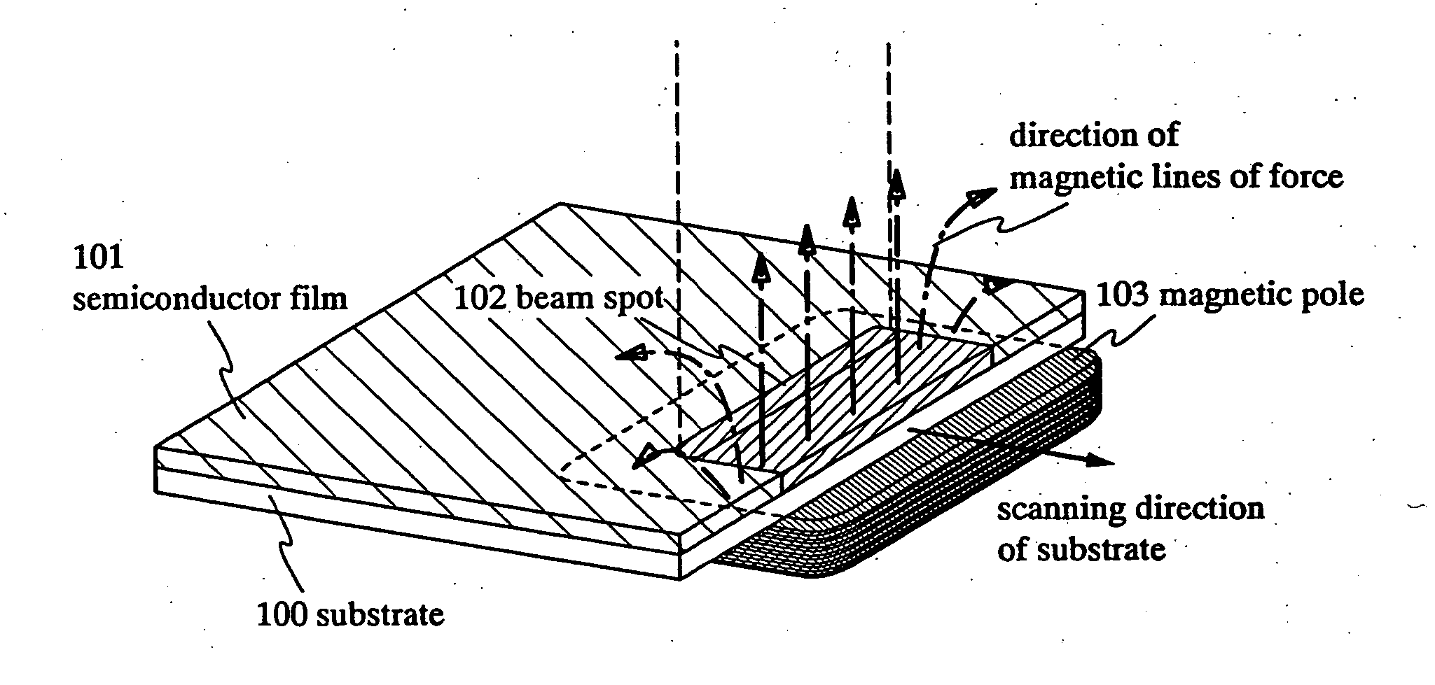
[0036] A laser irradiation method according to the present invention is explained with reference to FIG. 1. FIG. 1(A) shows an aspect in which a semiconductor film 101 formed over a substrate 100 is irradiated with the laser light. According to the present invention, before the crystallization by the irradiation of the laser light, the zeroth element, which is hard to form a chemical compound with semiconductor and which is neutral in the semiconductor so that it does not function as a dopant, is doped in the semiconductor film 101.

[0037] He, Ne, Ar, Kr, Xe, or the like is typically given as the doped zeroth element. As well as doping P or B imparting conductivity to the semiconductor film, the zeroth element can be doped by converting it into plasma and accelerating it by porous electrode. In addition, unlike P and B that are regulated legally, the above gases do not need to be diluted with hydrogen. As a result, throughput can be increased.

[0038] For example, ...

embodiment mode 2

[Embodiment Mode 2]

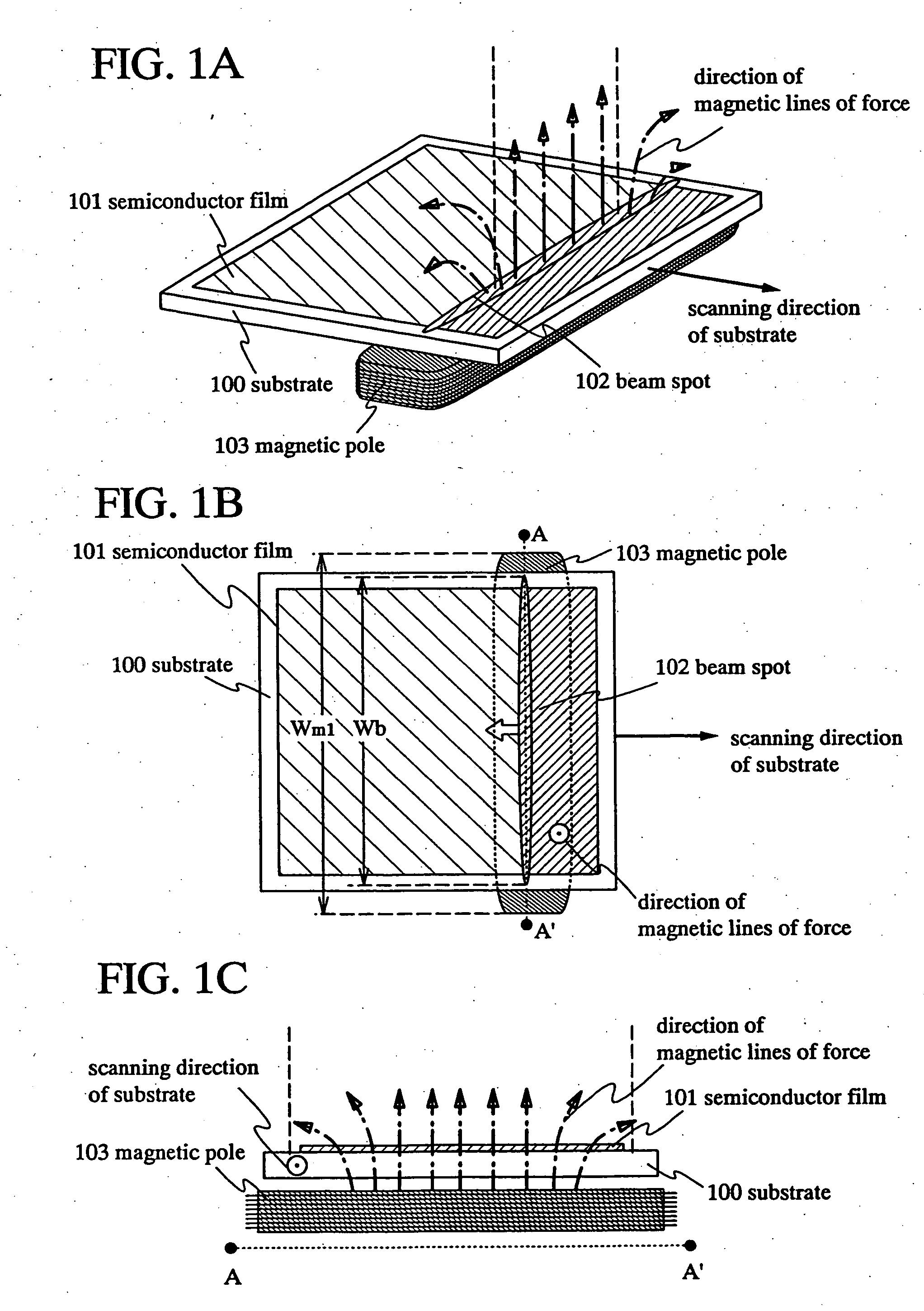
[0057] This embodiment mode explains one mode of the present invention where the magnetic field is applied to the direction different from that shown in FIG. 1 and FIG. 2.

[0058]FIG. 3(A) is a top view of the semiconductor film 201, and FIG. 3(B) is a cross-sectional view taken along the dotted line A-A′ in FIG. 3(A). It is noted that a reference numeral 201 corresponds to the semiconductor film formed over the substrate 200 in FIGS. 3(A) and 3(B).

[0059] The scanning direction of the substrate 200 exists in the surface of the substrate 200 as indicated by an arrow of a continuous line. In addition, a reference numeral 202 corresponds to the beam spot obtained by the pulsed laser light irradiated to the semiconductor film 201. The beam spot 202 to the semiconductor film 201 is moved relatively to the direction indicated by a white arrow by scanning the substrate 200 to the direction indicated by an arrow of a continuous line.

[0060] Magnetic poles 203a and 203b co...

embodiment mode 3

[Embodiment Mode 3]

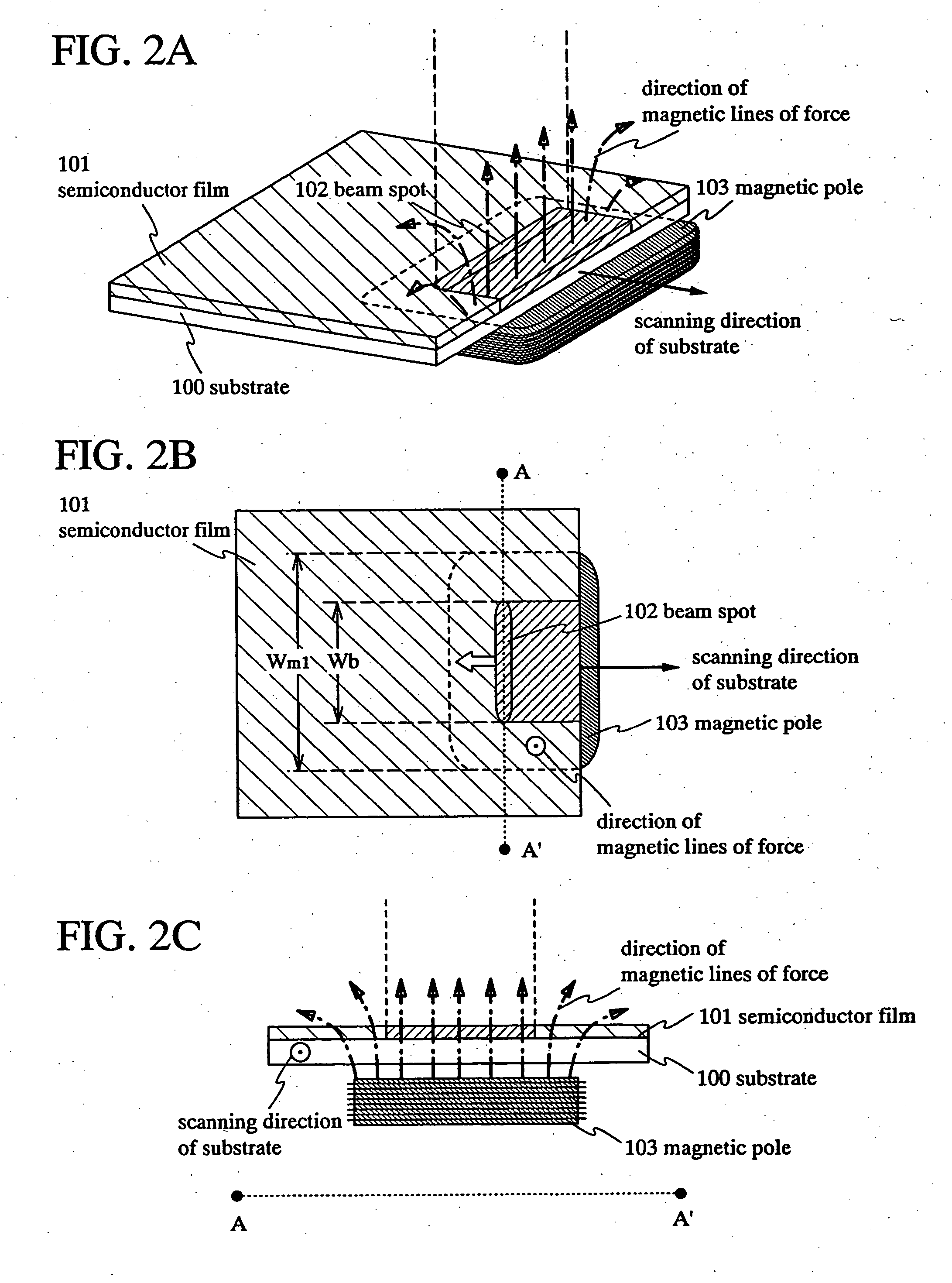
[0067] This embodiment mode explains one mode of the present invention in which the magnetic field is applied to the direction different from those in FIG. 1 to FIG. 4.

[0068]FIG. 5(A) is a top view of the semiconductor film 301 and FIG. 5(B) is a cross-sectional view taken along a dotted line A-A′ in FIG. 5(A). It is noted that a reference numeral 301 corresponds to a semiconductor film formed over a substrate 300 in FIGS. 5(A) and 5(B).

[0069] The scanning direction of the substrate 300 exists in the substrate 300 as indicated by an arrow of a continuous line. Moreover, a reference numeral 302 corresponds to the beam spot obtained by the pulsed laser light irradiated to the semiconductor film 301. The position of the beam spot 302 relatively to the semiconductor film 301 is moved to the direction indicated by a white arrow by scanning the substrate 300 in the direction indicated by an arrow of a continuous line.

[0070] The magnetic poles 303a and 303b correspond...


PUM

PropertyMeasurementUnit
magnetic fieldaaaaaaaaaa
drain currentaaaaaaaaaa
magnetic flux densityaaaaaaaaaa

Abstract

[Object]It is an object of the present invention to provide a laser irradiation apparatus being able to crystallize the semiconductor film homogeneously while suppressing the variation of the crystallinity in the semiconductor film and the unevenness of the state of the surface thereof. It is another object of the present invention to provide a method for manufacturing a semiconductor device using the laser irradiation apparatus which can suppress the variation of on-current, mobility, and threshold of TFT, and to further provide a semiconductor device manufactured with the manufacturing method. [Solution]A method for manufacturing a semiconductor device comprising the steps of adding the first noble gas to the semiconductor film formed over the insulating surface with the ion doping method and irradiating the semiconductor film with the first noble gas added therein with the laser light in an atmosphere of second noble gas, wherein the magnetic field is applied to the semiconductor film with the first noble gas added when the laser light is irradiated.

Description

TECHNICAL FIELD [0001] The present invention relates to a pulsed laser irradiation apparatus or a continuous wave laser irradiation apparatus, which is used for crystallizing a semiconductor film. In addition, the present invention relates to a method for manufacturing a semiconductor device including a process to crystallize a semiconductor film with the laser irradiation apparatus, and to a semiconductor device manufactured with the above manufacturing method. BACKGROUND ART [0002] Thin film transistor with a poly-crystalline semiconductor film (poly-crystalline TFT) is superior to TFT with an amorphous semiconductor film in its mobility by double digits or more. The poly-crystalline TFT has an advantage that a pixel portion and its peripheral driver circuit in a semiconductor display device can be integrated on the same substrate. [0003] The poly-crystalline semiconductor film can be formed over an inexpensive glass substrate when a laser annealing method is employed. However, th...

Claims


Application Information

Patent Timeline
Patent Type & Authority Applications(United States)
IPC IPC(8): H01L21/00C30B1/02C30B1/08H01L21/20
CPCC30B1/023C30B1/08H01L21/2026C30B29/06H01L21/02683H01L21/02686H01L21/02678H01L21/02488H01L21/02422H01L21/02532H01L21/0242H01L21/02672H01L21/02691
Inventor YAMAZAKI, SHUNPEINAKAMURA, OSAMUSHOJI, HIRONOBU
Owner SEMICON ENERGY LAB CO LTD
Why Eureka
Try Eureka