

Semiconductor device including active matrix circuit
a technology of active matrix circuit and semiconductor device, applied in non-linear optics, instruments, optics, etc., can solve the problems of not using the same structure to build, the register does not operate in the same way, etc., and achieves the effect of less deterioration in characteristics and reducing the steepness of steps
- Summary
- Abstract
- Description
- Claims
- Application Information
AI Technical Summary
Benefits of technology
Problems solved by technology
Method used
Image

Examples
first embodiment
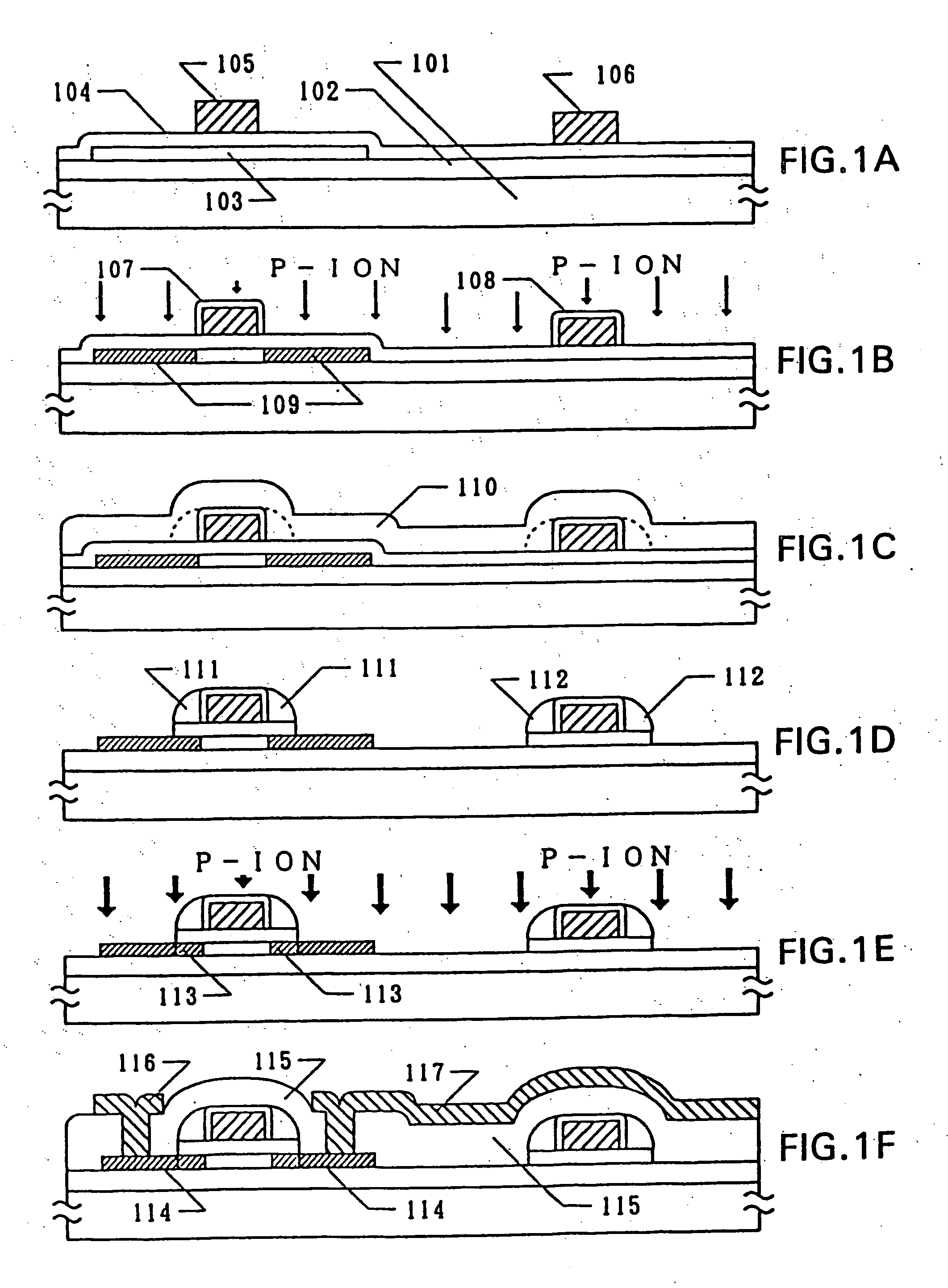
[0026]FIGS. 2A to 2G illustrate the present invention. A silicon oxide film having a thickness of 1000 to 5000 Å, e.g., 2000 Å, is formed as a base oxide film 202 on a substrate (Corning 7059) 201. This oxide film is formed using a sputtering process in an oxygen atmosphere. For higher mass-productivity, it may be formed by decomposing and depositing TEOS (tetraethoxysilane) using a plasma CVD process. The silicon oxide film thus formed may be annealed at 400 to 650° C.
[0027] Thereafter, an amorphous silicon film is deposited using a plasma CVD process or LPCVD process to a thickness of 300 to 5000 Å, preferably 400 to 1000 Å, e.g., 500 Å. The film is then crystallized by keeping it in a reducing atmosphere at 550 to 600° C. for 8 to 24 hours. The crystallization may be accelerated (promoted) by adding a very small amount of metal element such as nickel which promotes the crystallization. Alternatively, this process may be carried out using laser irradiation. The resulting crystalli...
second embodiment
[0042] the present invention will now be described.
[0043] This embodiment relates to a monolithic active matrix circuit which is schematically shown FIGS. 4A to 4C. The elements in this embodiment are constructed in a manner which is basically the same as that in the first embodiment. The present embodiment is an improvement over the monolithic active matrix circuit shown at FIG. 2G.
[0044] Transistors 401 and 402 are of the N-channel type and P-channel type, respectively, and are both used in a peripheral driving circuit. The peripheral driving circuit has a contact portion 403 for establishing contact between the gate line and a line 404 of a second layer. The contact hole is formed in both of the layer insulator and anodic oxide. (See FIG. 4A)
[0045] A circuit diagram of a unit pixel of the active matrix circuit is shown in FIG. 4C. The present embodiment employs a double gate circuit wherein transistors 405 and 406 are connected in series as a switching element. A line 407 which...
third embodiment
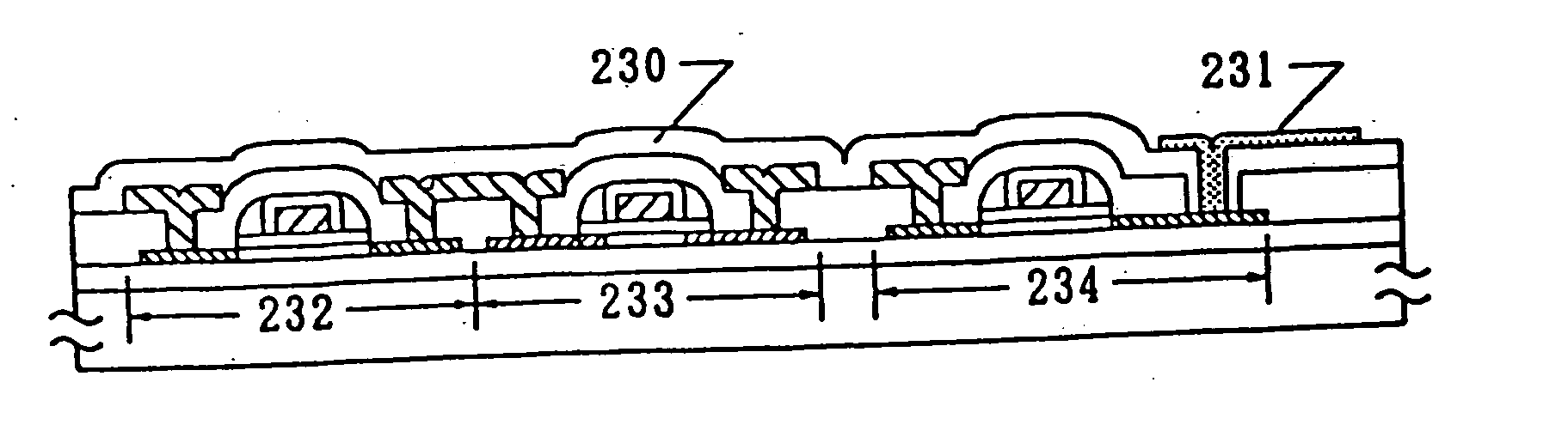
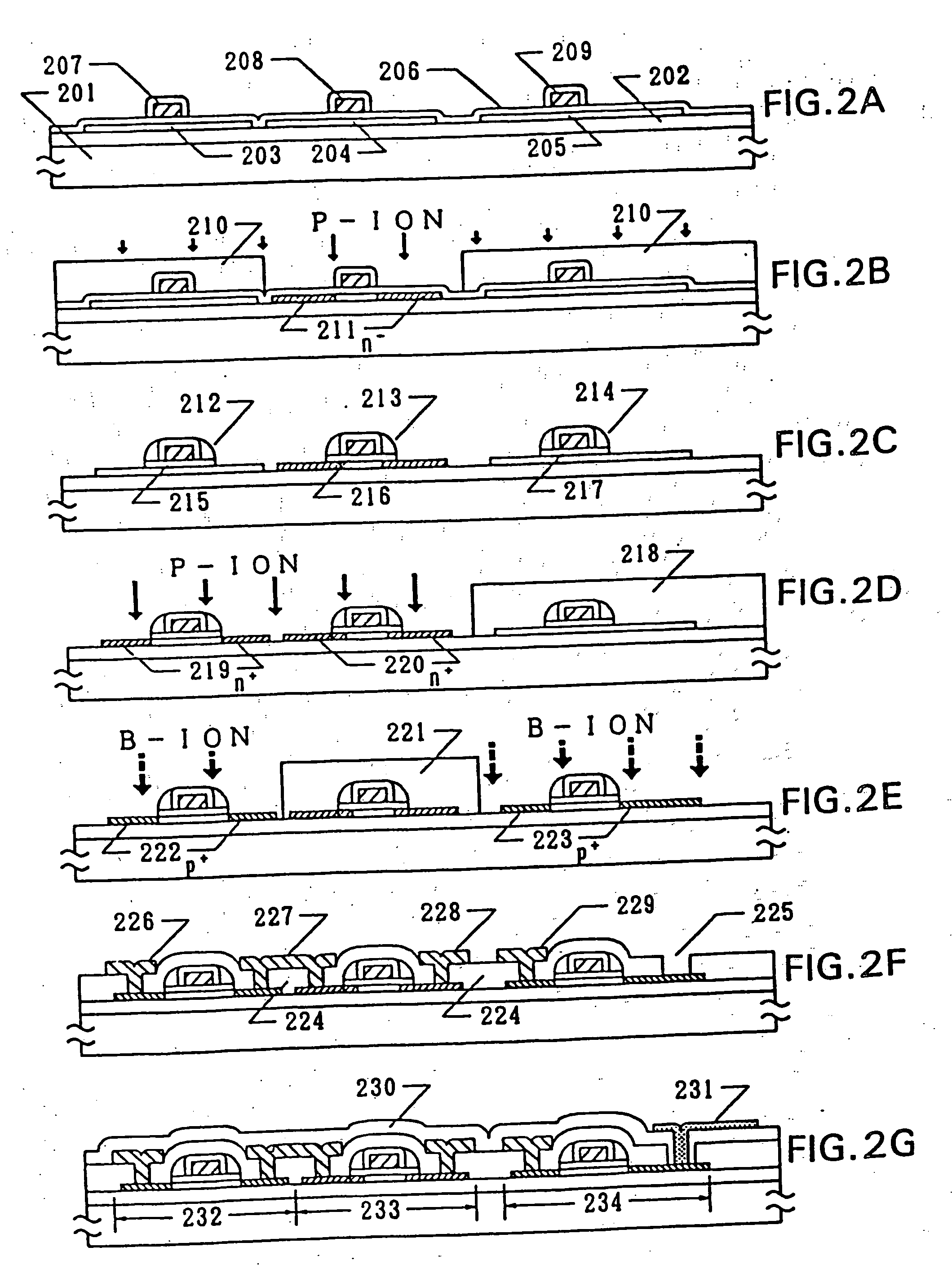
[0046]FIGS. 3A to 3G illustrate the present invention. Crystalline island-like silicon regions 303, 304, and 305 are formed on a substrate 301 on which a silicon oxide film having a thickness of 2000 Å is formed as a base oxide film 302. In addition, a silicon oxide film 306 having a thickness of 1200 Å is formed thereon using a plasma CVD process. The island-like regions 303 and 304 represent TFTs for peripheral circuits of the active matrix circuit, whereas the island-like region 305 represents a region in which a TFT for the active matrix circuit is formed. Further, aluminum gate electrodes 307, 308, and 309 are formed which are 5000 Å thick and are anodized on the side and upper surfaces thereof. (See FIG. 3A)
[0047] Thereafter, the regions 303 and 305 in which P-channel type TFTs are to be formed are covered with photoresist masks 310. Phosphorous is implanted in the island-like silicon film 304 on a self-alignment basis using the gate electrode portion as a mask according to th...
PUM
| Property | Measurement | Unit |
|---|---|---|
| current | aaaaa | aaaaa |
| voltage | aaaaa | aaaaa |
| current | aaaaa | aaaaa |
Abstract
Description
Claims
Application Information