Nanocrystal silicon quantum dot memory device

a quantum dot and quantum dot technology, applied in semiconductor devices, digital storage, instruments, etc., can solve the problems of cell wear, flash memory wear factor, non-uniformity of insulating oxides, etc., and achieve the effect of reducing the thickness of tunnel oxide and inter-level oxides, and sacrificing memory retention tim

Inactive Publication Date: 2007-05-17
SHARP LAB OF AMERICA INC
View PDF4 Cites 18 Cited by
  • Summary
  • Abstract
  • Description
  • Claims
  • Application Information

AI Technical Summary

Benefits of technology

[0011] If the floating gate of a flash memory is replaced with nano particles, a weak spot in an insulating oxide layer only affects one adjacent nano particle, and has no effect on the other storage particles. Therefore, the thickness of both the tunnel (gate) oxide and the inter-level (control) oxide can be reduced, without sacrificing the memory retention time. The present invention provides multi-layer chemical vapor deposition (CVD) poly-Si and thermal oxidation processes for fabricating a nano-Si quantum dots flash memory that addresses the issue of weakness in an insulating oxide.

Problems solved by technology

One of the primary problems with this type of memory is that the cells “wear out” after many erase operations, due to wear on the insulating or tunneling oxide layer around the charge storage mechanism used to store data.
As noted above, a fundamental problem associated with flash memory is the wear factor.
This problem is typically due to the non-uniformity of the insulating oxide.
If there is a weak spot, such that the leakage current density at that spot is larger than in the adjacent areas, all of the stored charges in the floating gate are liable to leak.
This problem increases with the thinning of the oxide thickness.
Thus, it is difficult to reduce the size, or increase the density of a flash memory.

Method used


Image

  • Nanocrystal silicon quantum dot memory device
  • Nanocrystal silicon quantum dot memory device
  • Nanocrystal silicon quantum dot memory device

Examples


Embodiment Construction

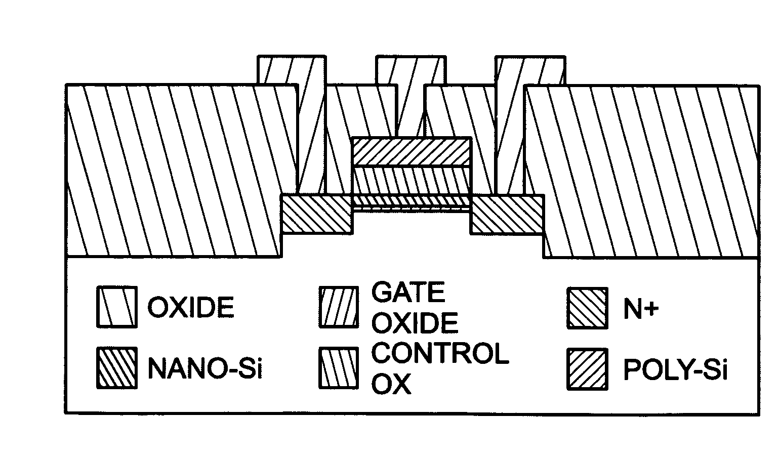
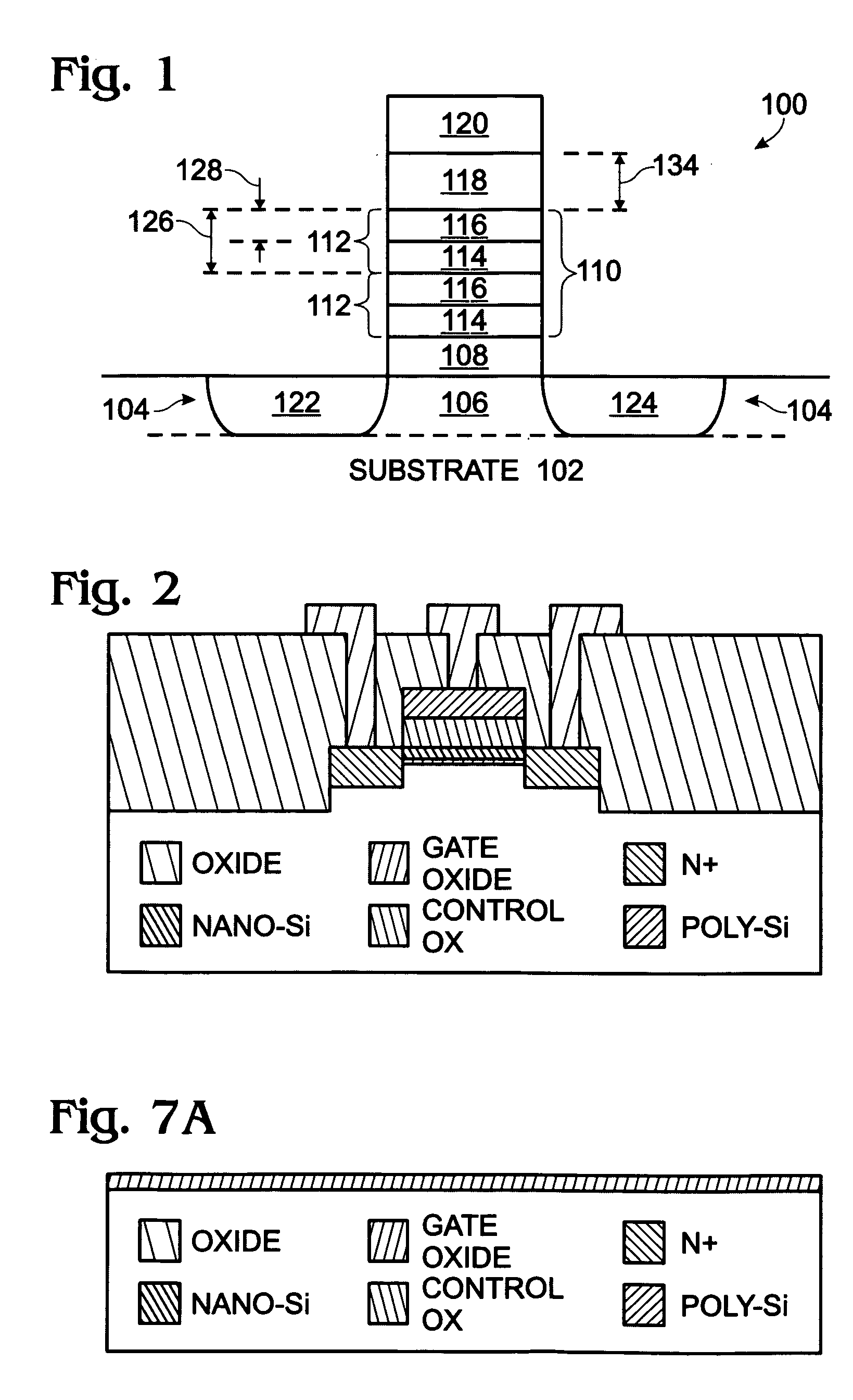
[0034]FIG. 1 is a partial cross-sectional view of a nanocrystal silicon (Si) quantum dot memory device. The memory device 100 comprises a Si substrate 102 having a Si active layer 104 with a channel region 106, as is conventional with an MOSFET device. A gate oxide layer 108 overlies the channel region 106. The gate oxide layer 108 is also referred to a tunneling oxide layer. A nanocrystal Si film 110, which is referred to herein as a memory film, overlies the gate oxide layer 108. The nanocrystal Si memory film 110 is also known as a floating gate (FG). The nanocrystal Si memory film 110 includes at least one polycrystalline Si (poly-Si) / Si dioxide stack 112, where each stack includes a poly-Si layer 114 and a Si dioxide layer 116.

[0035] A control Si oxide layer 118 overlies the nanocrystal Si memory film 110. A gate electrode 120, or control gate (CG), overlies the control oxide layer 118. The gate electrode 120 can be poly-Si or a metal, for example. As is conventional, source / d...


PUM

PropertyMeasurementUnit
thicknessaaaaaaaaaa
temperatureaaaaaaaaaa

Abstract

A nanocrystal silicon (Si) quantum dot memory device and associated fabrication method have been provided. The method comprises: forming a gate (tunnel) oxide layer overlying a Si substrate active layer; forming a nanocrystal Si memory film overlying the gate oxide layer, including a polycrystalline Si (poly-Si)/Si dioxide stack; forming a control Si oxide layer overlying the nanocrystal Si memory film; forming a gate electrode overlying the control oxide layer; and, forming source/drain regions in the Si active layer. In one aspect, the nanocrystal Si memory film is formed by depositing a layer of amorphous Si (a-Si) using a chemical vapor deposition (CVD) process, and thermally oxidizing a portion of the a-Si layer. Typically, the a-Si deposition and oxidation processes are repeated, forming a plurality of poly-Si/Si dioxide stacks (i.e., 2 to 5 poly-Si/Si dioxide stacks).

Description

BACKGROUND OF THE INVENTION [0001] 1. Field of the Invention [0002] This invention generally relates to integrated circuit (IC) fabrication and, more particularly, to a flash memory device that uses a nanocrystalline quantum dot memory film. [0003] 2. Description of the Related Art [0004] Flash memory is non-volatile, which means that it does not need power to maintain its memory state. Flash memory offers relatively fast read access times, and is more shock resistant than a hard disk. A typical flash memory system only permits one location at a time to be erased or written. Therefore, higher overall speeds are obtained when the system architecture permits multiple reads to take place simultaneous with a single write. [0005] Flash memory comes in two forms, either NOR or NAND flash, referring to logic gate used in each cell. One of the primary problems with this type of memory is that the cells “wear out” after many erase operations, due to wear on the insulating or tunneling oxide ...

Claims


Application Information

Patent Timeline
Patent Type & Authority Applications(United States)
IPC IPC(8): H01L29/788H01L21/336G11C16/04
CPCB82Y10/00G11C16/349G11C16/3495G11C2216/08H01L21/28273H01L29/15H01L29/42324H01L29/4925H01L29/66825H01L29/7881H01L29/40114
Inventor LI, TINGKAIHSU, SHENG TENGSTECKER, LISA H.
Owner SHARP LAB OF AMERICA INC
Why Eureka
Try Eureka