Method of defining semiconductor fabrication process utilizing transistor inverter delay period

a semiconductor fabrication and delay period technology, applied in the field of data communication, can solve the problems of minute inherent inconsistencies among chips, longer test times, and a particularly vexing challenge for designers of high-end devices, and achieve the effect of improving silicon performan

Active Publication Date: 2007-05-17
DE OBALDIA ELIDA ISABEL +3
View PDF5 Cites 34 Cited by
  • Summary
  • Abstract
  • Description
  • Claims
  • Application Information

AI Technical Summary

Benefits of technology

[0013] As compared to when wafers processes had been measured using prior art methods, using the information provided by the inverter delay was found to be directly proportional to the process variation of the tested core transistors, in examples where channel dimension variation was known to correspond to transistor strength. Knowing how the process varies, allows adjustments to be made in the application software to improve the silicon performance.
[0017] Several advantages of the process corner measurement of the present invention include: (1) direct measurement of the transition delay (which is inversely proportional to the period inversion) of the core NMOS / PMOS transistor-based inverter used in the chip; (2) transition delay is proportional to the NMOS and PMOS process strength; (3) no external equipment is required to perform this measurement as it is already implemented in the ADPLL circuit; and (4) the process knowledge is used to take full advantage of the software controlled radio (i.e. DRP) by providing the basis for process parameter compensation.

Problems solved by technology

In the fabrication of DRPs and other CMOS ICs it is well known that process variation in the core transistor for RF-CMOS technology results from minute inherent inconsistencies among chips made even within a single batch made from a few wafers or even a single wafer.
This variation presents a particularly vexing challenge for designers of highly integrated “systems on a chip” (SoC).
Unfortunately, indirect and external measurement to deduce process variation requires additional costly equipment and steps in the manufacturing process resulting in longer test times and significantly higher costs.
Using an external test equipment would be inconvenient or impossible at certain stages of IC lifecycle, such as after the IC is assembled or in customer hands.

Method used


Image

  • Method of defining semiconductor fabrication process utilizing transistor inverter delay period
  • Method of defining semiconductor fabrication process utilizing transistor inverter delay period
  • Method of defining semiconductor fabrication process utilizing transistor inverter delay period

Examples


Embodiment Construction

Notation Used throughout

[0037] The following notation is used throughout this document.

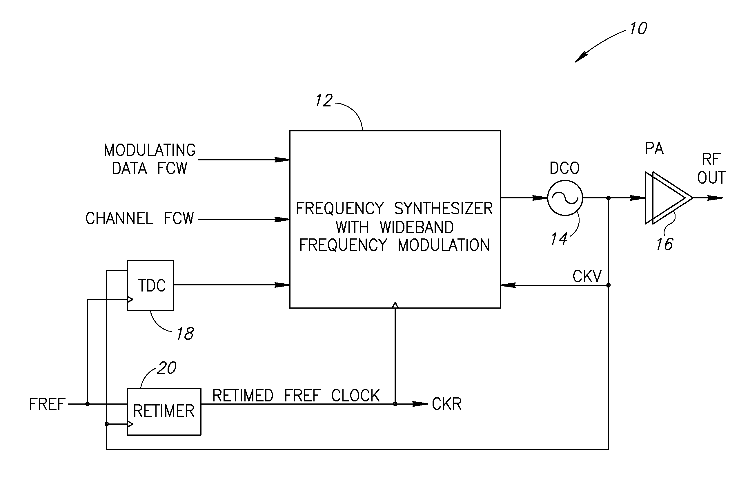
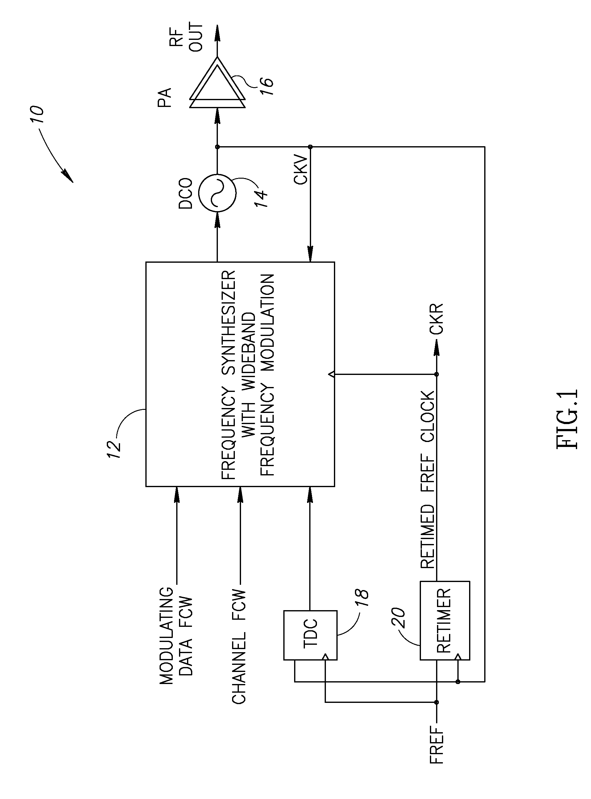
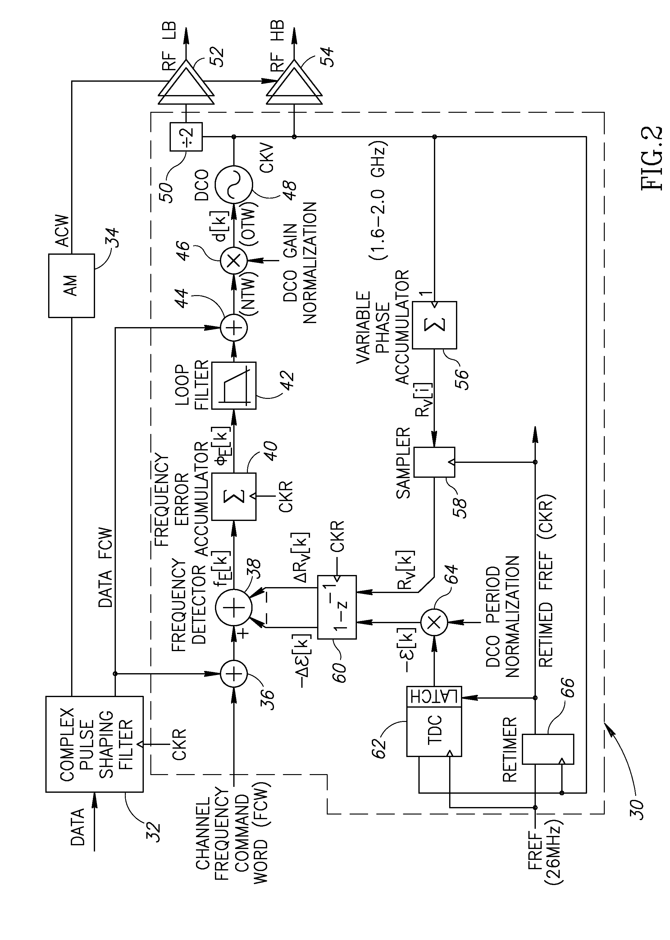
TermDefinitionACWAmplitude Control WordADCAnalog to Digital ConverterADPLLAll Digital Phase Locked LoopAMAmplitude ModulationASICApplication Specific Integrated CircuitCDMACode Division Multiple AccessCKRRetimed Reference ClockCKVVariable Oscillator ClockCMOSComplementary Metal Oxide SemiconductorDACDigital to Analog ConverterDCODigital Controlled OscillatorDCSDigital Communication ServicesDCXODigitally Controlled Crystal OscillatorDEMDynamic Element MatchingDOEDesign of ExperimentsDRPDigital RF Processor or Digital Radio ProcessorDSPDigital Signal ProcessorFCWFrequency Command WordFPGAField Programmable Gate ArrayFREFFrequency ReferenceGSMGlobal System for Mobile CommunicationHBHigh BandHDLHardware Description LanguageICIntegrated CircuitIFIntermediate FrequencyIIRInfinite Impulse ResponseLBLow BandLDOLow Drop Out regulatorLNALow Noise AmplifierLOLocal OscillatorLUTLook Up TablePAPower Amplifi...


PUM


Abstract

A novel method and apparatus for defining process variation in a digital RF processor (DRP). The invention is well suited for use in highly integrated system on a chip (SoC) radio solutions that incorporate a very large amount of digital logic circuitry. The method and apparatus provide direct measurement of fabrication process variation in circuits without requiring any additional test equipment by utilizing a time to digital converter (TDC) circuit already present in the chip. The TDC circuit relies on the time delay in an inverter chain to sample a high speed CKV clock using a slow FREF clock. Calculation of inverse time provides a direct correlation for fabrication process variation in each die.

Description

REFERENCE TO PRIORITY APPLICATION [0001] This application claims priority to U.S. Provisional Application Ser. No. 60 / 728,395, filed Oct. 19, 2005, entitled “Fab process definition by calculating transistor invert delay period with TDC,” incorporated herein by reference in its entirety.FIELD OF THE INVENTION [0002] The present invention relates to the field of data communications and more particularly relates to a method for defining the semiconductor fabrication process by measuring inverter delay. BACKGROUND OF THE INVENTION [0003] Complementary Metal Oxide Semiconductor (CMOS) technology has recently evolved, in terms of both frequency and noise, where it is increasingly being used in radio frequency (RF) applications in the GHz frequency range. Currently, cutoff frequencies of over 50 GHz have been reported for 0.18 μm CMOS technology and are expected to reach as high as 100 GHz as feature size shrinks to 100 nm. This translates into CMOS circuit operating frequencies well into ...

Claims


Application Information

Patent Timeline
Patent Type & Authority Applications(United States)
IPC IPC(8): H04L27/08H03L7/00
CPCH03L7/091H03L7/0991H03L7/1806H04L27/361
Inventor DE OBALDIA, ELIDA ISABELSTASZEWSKI, ROBERT B.LEIPOLD, DIRK
Owner DE OBALDIA ELIDA ISABEL
Why Eureka
Try Eureka