

Display device and electronic device
- Summary
- Abstract
- Description
- Claims
- Application Information
AI Technical Summary
Benefits of technology
Problems solved by technology
Method used
Image

Examples
embodiment mode 1
(Circuit Configuration 1)
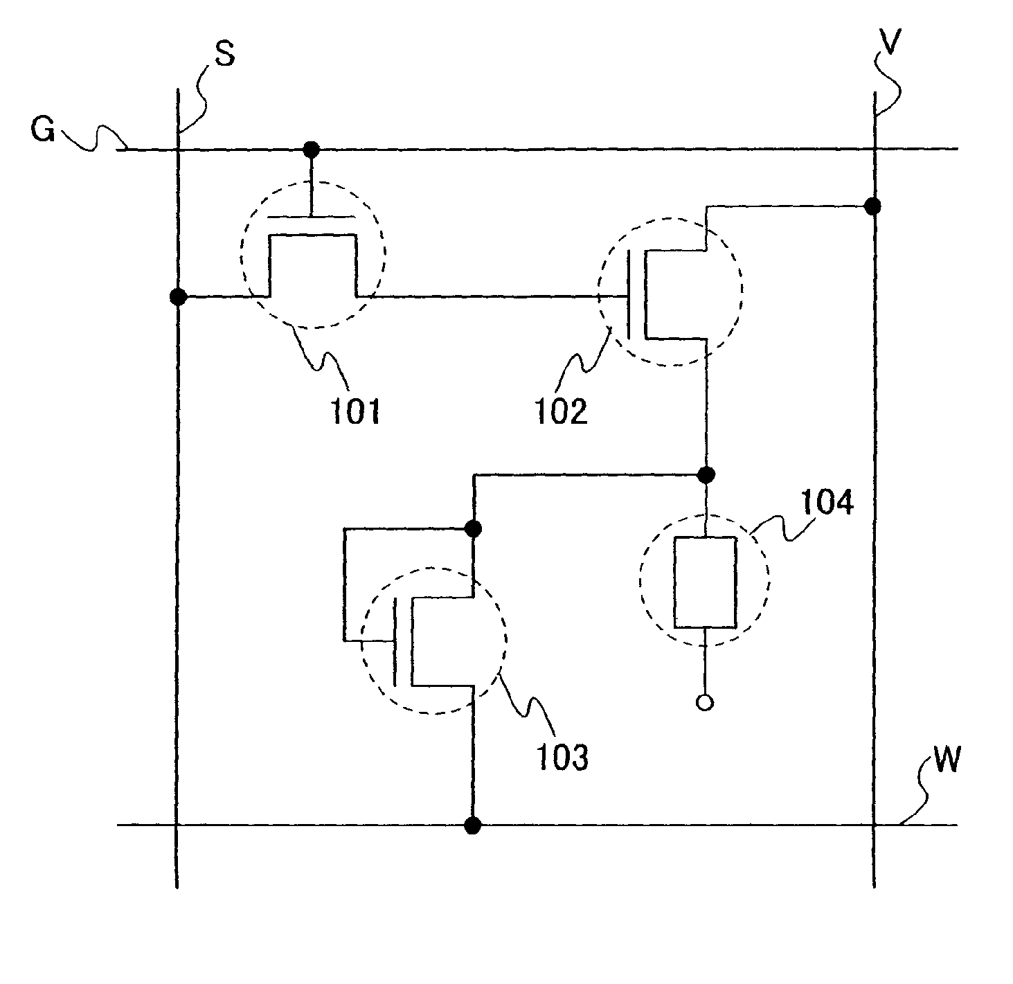
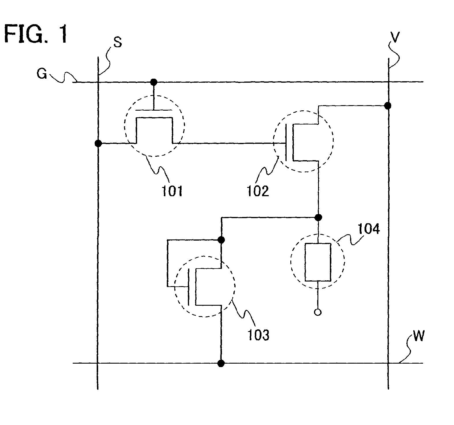
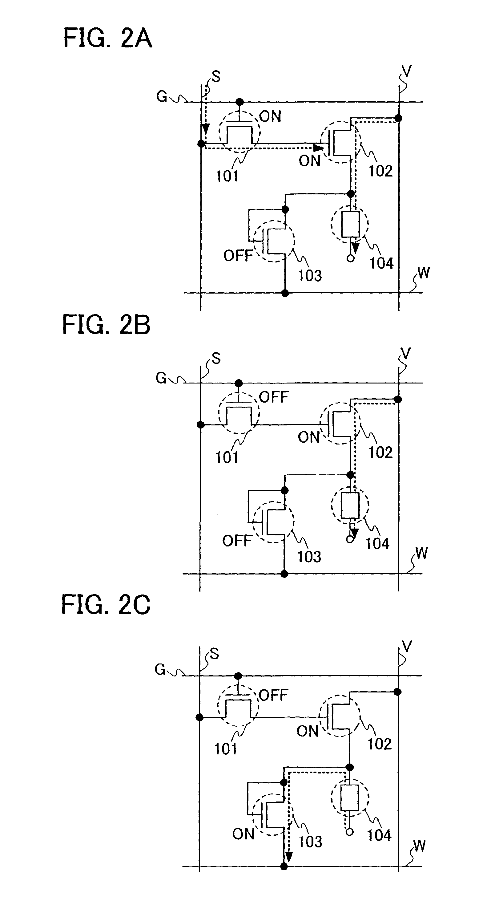
[0086] In FIG. 1, an embodiment mode of a circuit constituting a pixel is shown as a circuit configuration (also referred to as a pixel configuration) diagram of the present invention.
[0087] A circuit constituting a pixel shown in FIG. 1 includes a light emitting element 104, a transistor used as a switching element for controlling the input of a video signal to the pixel (a switching transistor 101), a transistor that controls the value of a current flowing to the light emitting element 104 (a driving transistor 102), and a transistor that applies a reverse bias current to the light emitting element 104 when a reverse voltage is applied to the light emitting element 104 (an AC transistor 103). The switching transistor 101, the driving transistor 102, and the AC transistor 103 have the same conductivity type, and an N-type transistor is used for each of these transistors, which is a characteristic of the present invention. Although a capacitor element is ...
embodiment mode 2
[0138] In this embodiment mode, a structure of a display, constituting the display device which is manufactured using Embodiment Mode 1 described above, will be described.
[0139] The display device includes a display and a peripheral circuit which inputs a signal to the display.
[0140] A block diagram of a display structure is shown in FIG. 5. In FIG. 5, a display 300 includes a signal line driver circuit 301, a scanning line driver circuit 302, and a pixel portion 303. The pixel portion 303 has a structure in which pixels are arranged in a matrix.
[0141] A thin film transistor (hereinafter referred to as a TFT) is placed in each pixel in the pixel portion 303. Here, a description will be made of a display in which three TFTs are arranged for each pixel, using the circuit configuration described in Embodiment Mode 1 above, and in which a light emitting element is provided in each pixel.
[0142] A structure of the pixel portion in the display is shown in FIG. 6. In the pixel portion 3...
embodiment mode 3
(Circuit Configuration 2)
[0146] In this embodiment mode, a configuration different from the circuit configuration of FIG. 1 described in Embodiment Mode 1 will be described.
[0147] A circuit constituting a pixel shown in FIG. 7 includes a light emitting element 104, a transistor used as a switching element for controlling the input of a video signal to a pixel (a switching transistor 101), a transistor that controls the value of a current flowing to the light emitting element 104 (a driving transistor 102), and a transistor that applies a reverse bias current to the light emitting element 104 when a reverse voltage is applied to the light emitting element 104 (an AC transistor 103). The switching transistor 101, the driving transistor 102, and the AC transistor 103 have the same conductivity type, and an N-type transistor is used for each of these transistors, which is a characteristic of the present invention. Although a capacitor element is not provided in this embodiment mode, ...
PUM
 Abstract
Description
Claims
Application Information