Method for manufacturing semiconductor device and semiconductor device

Active Publication Date: 2007-06-07
RENESAS ELECTRONICS CORP
View PDF6 Cites 13 Cited by
  • Summary
  • Abstract
  • Description
  • Claims
  • Application Information

AI Technical Summary

Benefits of technology

[0038] The polycrystalline silicon film 110 may be formed via, for example, a chemical vapor deposition (CVD) process or the like.
[0039] Subsequently, an annealing process may be conducted at a temperature around 500 degree C. for about several minutes, so that a counter diffusion of the metal of the first metallic film 108 and silicon (Si) of the polycrystalline silicon film 110 is created, thereby forming a first silicide layer 110a in the lower portion of the polycrystalline silicon film 110 (FIG. 1B). The component of such first silicide layer 110a may be represented as MxSi (where M is a metallic element selected from Ni, Co, W and Ti, and x is a number of not less than 1). Having such component, a generation of Fermi level pinning can be further inhibited, so that a variation in threshold voltage can be effectively inhibited.
[0040] Then, a lithographic process and a reactive ion etching (RIE) process are conducted to form a gate electrode, and further an extension region 118, a side wall 120 and a source/drain region 122 are formed according to an ordinary process (FIG. 2A).
[0041] Subsequently, a second metallic film is formed on the entire wafer surface via a sputter process or the like. Then, the polycrystalline silicon film 116 and the source/drain region 122 are silicidized by the presence of the second metallic film 124 and 12

Problems solved by technology

In this case, an insufficient diffusion of a metal around the gate insulating film may cause a silicon (Si)-rich condition in the gate insulating film side of the gate electrode, causing a generation of Fermi l

Method used


Image

  • Method for manufacturing semiconductor device and semiconductor device
  • Method for manufacturing semiconductor device and semiconductor device
  • Method for manufacturing semiconductor device and semiconductor device

Examples


first embodiment

[0033] In first embodiment, a case of forming an n-type metal oxide semiconductor field effect transistor (MOSFET) will be described.

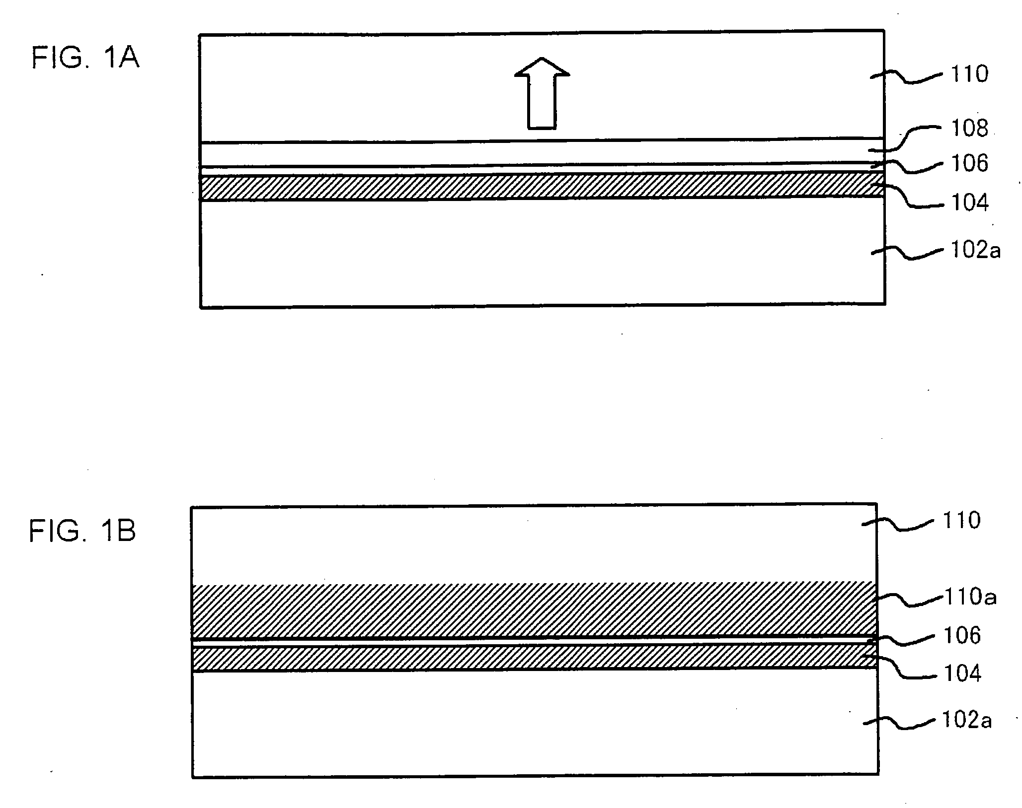
[0034] First of all, as shown in FIG. 1A, a gate insulating film 104, a barrier film 106, a the first metallic film 108 and a polycrystalline silicon film 110 are sequentially deposited on a p-type semiconductor substrate 102a.

[0035] The gate insulating film 104 may be composed of a high dielectric constant film containing one or more metallic element(s) selected from a group consisting of Hf, Zr, Al, La and Ta. More specifically, typical high dielectric constant films may include hafnium oxide (HfO2) film, zirconium oxide (ZrO2) film, aluminum oxide (Al2O3) film, lanthanum oxide (LaO2) film, tantalum oxide (Ta2O5) films or the like. The gate insulating film 104 may be formed by conducting about 20 cycles of a deposition process via, for example, an atomic layer deposition (ALD) process. The thickness of the gate insulating film 104 may be about 3 nm...

second embodiment

[0049] In the second embodiment, a formation of an n-type MOSFET and a p-type MOSFET, which are arranged to be adjacent, will be illustrated. In the following discussions, an n-type MOSFET forming region includes both a region where an n-type MOSFET is to be formed and a region where an n-type MOSFET has been formed. Further, a p-type MOSFET forming region includes both a region where a p-type MOSFET is to be formed and a region where a p-type MOSFET has been formed.

[0050] First of all, a semiconductor substrate 102 is prepared, in which a p-type semiconductor substrate 102a is isolated from an n-type semiconductor substrate 102b by an element isolation film 130.

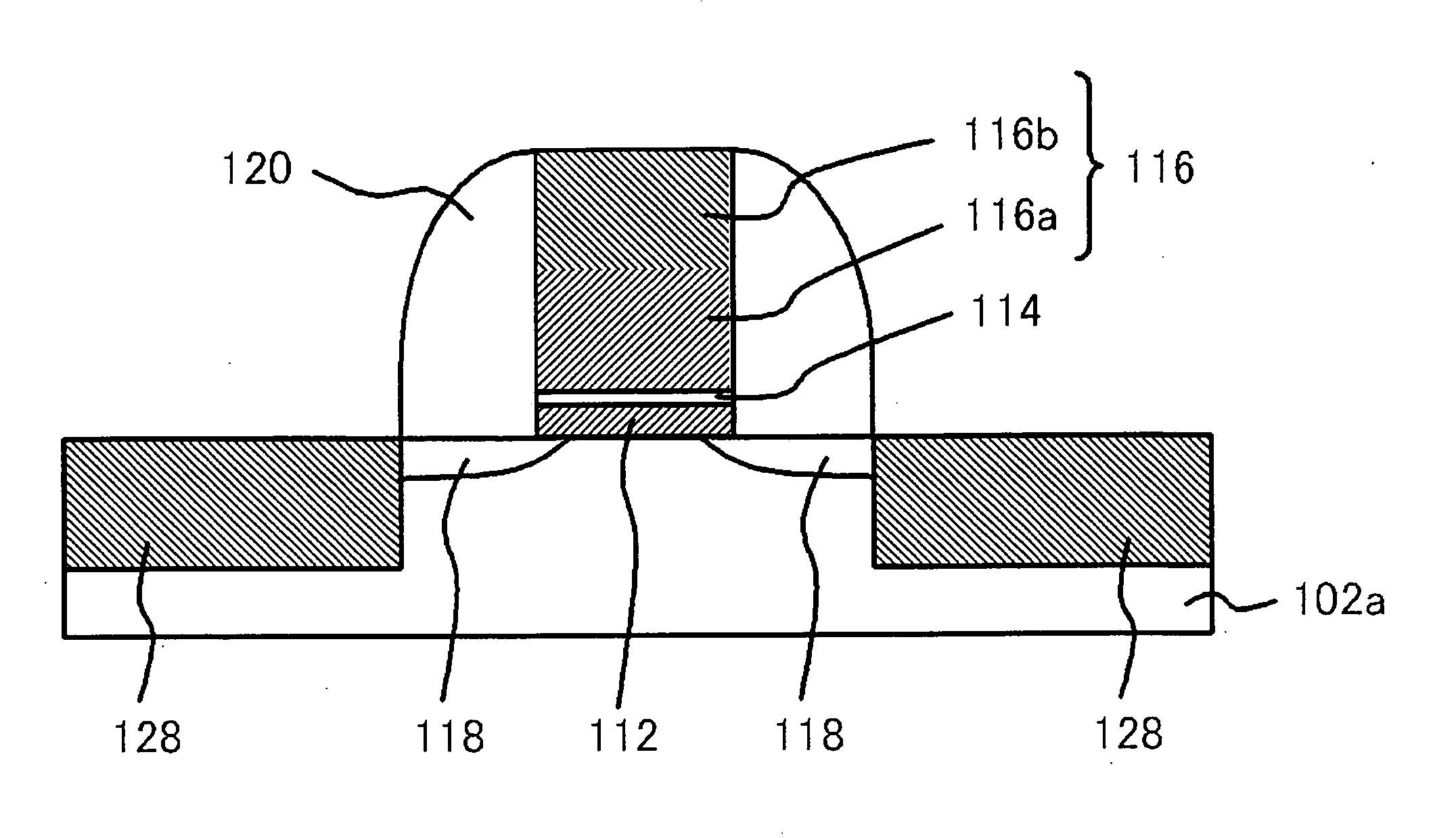
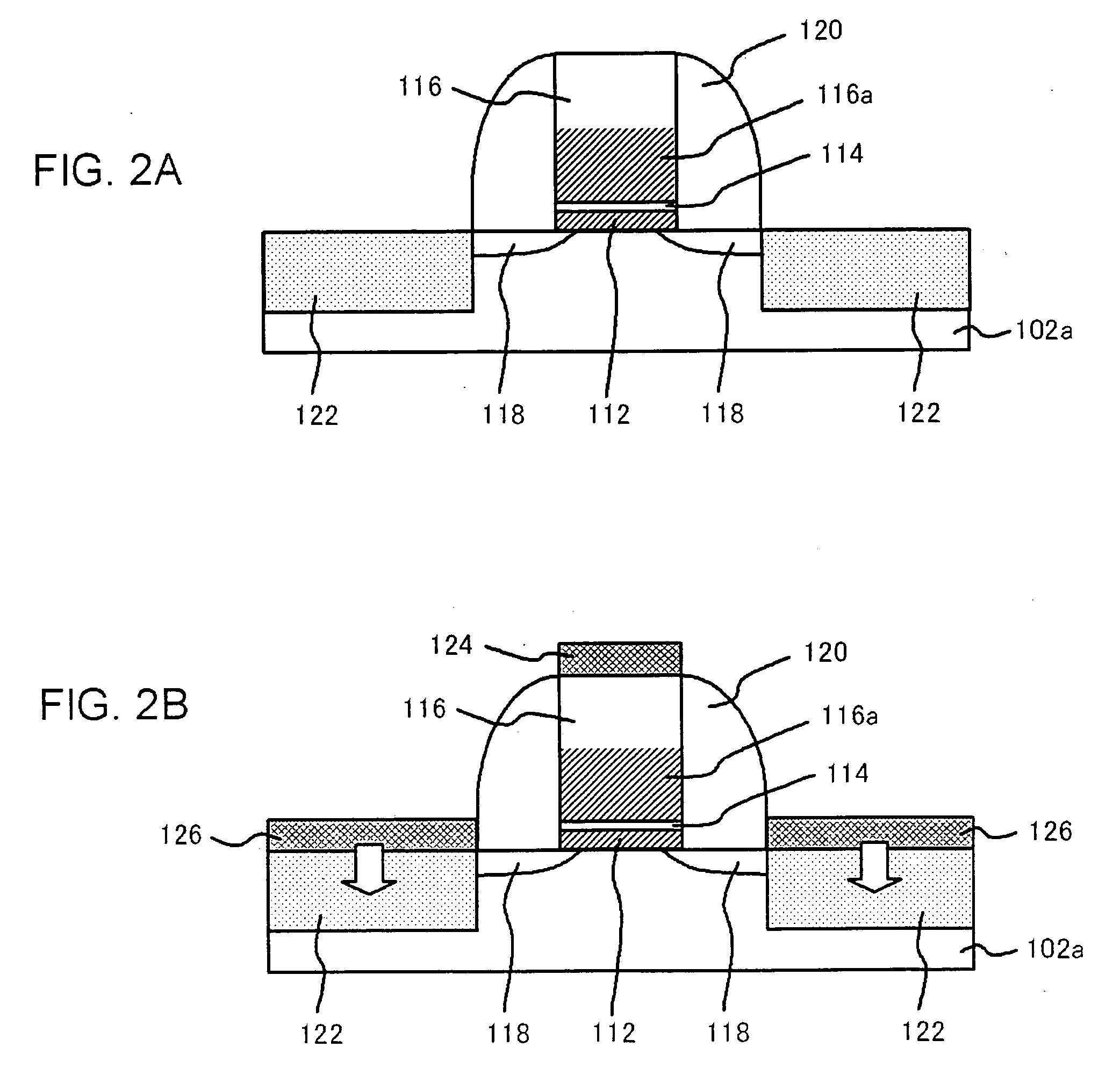
[0051] In an n-type MOSFET forming region, a gate electrode having a gate insulating film 112, a barrier film 114 and a polycrystalline silicon film 116 having a first silicide layer 116a in the lower portion are deposited on the p-type semiconductor substrate 102a, is formed via a process similar as the process employed i...

example 1

[0067] A semiconductor device was manufactured by a method similar as employed in first embodiment (FIG. 1 to FIG. 3). Manufacture conditions and configuration of a semiconductor device are described below: [0068] gate insulating film 104: HfO2 film, film thickness of 4 nm (deposited by 20 cycle of ALD processes); [0069] barrier film 106: TiN film, film thickness of 1 nm (deposited by 5 cycle of ALD processes); [0070] first metallic film 108: Ni film (deposited by sputter process); [0071] polycrystalline silicon film 110: deposited by CVD process; [0072] second metallic films 124 and 126: W film (deposited by sputter process); [0073] condition for forming the first silicide layer 110a: annealing at around 500 degree C. for 5 minutes; and [0074] condition for forming the second silicide layer 116b: annealing at around 650 degree C. for 5 minutes.


PUM


Abstract

Method for manufacturing a semiconductor device, capable of providing a reduced variation in threshold electrical voltage by inhibiting a generation of Fermi level pinning, while achieving a stable long-term reliability of a product by inhibiting a generation of leakage current, and such semiconductor device. The method includes: forming a gate electrode by: sequentially depositing a gate insulating film composed of a high dielectric constant film containing one or more metallic element(s) selected from Hf, Zr, Al, La and Ta, a barrier film composed of one or more metal nitride selected from TiN, TaN and WN, a metallic film 108 and a polycrystalline silicon film on the semiconductor substrate to form a multiple-layered film; and silicidizing a lower portion of the polycrystalline silicon film to form a lower layer by conducting a heat treatment of the multiple-layered film to diffuse the metal of the metallic film into the polycrystalline silicon film.

Description

[0001] This application is based on Japanese patent application No. 2005-351,830, the content of which is incorporated hereinto by reference. BACKGROUND [0002] 1. Technical Field [0003] The present invention relates to a method for manufacturing a semiconductor device by silicidizing a lower portion of a polycrystalline silicon film that composes a gate electrode, and to a semiconductor device. [0004] 2. Related Art [0005] A semiconductor device having a metallic gate electrode, all of which are silicidized, is developed. A typical process for manufacturing such type of semiconductor device is disclosed by, for example, T. Nabatame et al., IEDM Tech. Dig., pp. 83 (2004). [0006] The manufacturing process of T. Nabatame et al. involves, as shown in FIG. 6, growing a gate insulating film 14 composed of a high dielectric constant film (hereinafter referred to as high-k film) composed of hafnium oxide (HfO2) or the like on a semiconductor substrate 12 via an atomic layer deposition (ALD)...

Claims


Application Information

Patent Timeline
IPC IPC(8): H01L21/8244H01L29/94
CPCH01L21/28088H01L21/28194H01L21/823443H01L21/82345H01L21/823835H01L21/823842H01L29/4966H01L29/517H01L29/665H01L29/6659
Inventor IWAKI, TAKAYUKI
Owner RENESAS ELECTRONICS CORP
Why Eureka
Try Eureka