Method of manufacturing organic light emitting device and vapor deposition system

a technology of light emitting devices and vapor deposition systems, which is applied in the direction of vacuum evaporation coatings, chemical vapor deposition coatings, coatings, etc., can solve the problems of insufficient function as donor dopants, increased drive voltage, and low drive voltage, and achieve low voltage and high electron injection efficiency

Inactive Publication Date: 2007-06-14
CANON KK
View PDF16 Cites 8 Cited by
  • Summary
  • Abstract
  • Description
  • Claims
  • Application Information

AI Technical Summary

Benefits of technology

[0008] In view of the above, an object of the present invention is to provide a method of manufacturing an organic light emitting device which has high electron injection efficiency and can be driven at a low voltage, and to provide a vapor deposition system.
[0011] According to the present invention, the electron-injecting dopant in the electron injection layer can be caused to function more efficiently. As a result, the organic light emitting device manufactured according to the present invention has high electron injection efficiency and can be driven at a low voltage. Further, according to the present invention, continuous production over a long period of time without deteriorating device characteristics can be carried out.

Problems solved by technology

However, according to the technology disclosed in Japanese Patent Application Laid-Open Nos. 2000-182774, 2004-311403, and 2005-123094, when the metal compound is not reduced and remains in an organic film, it does not sufficiently function as a donor dopant, and even if a doping concentration is improved, drive voltage is not lowered.
On the contrary, there is a possibility that the drive voltage may rise.

Method used


Image

  • Method of manufacturing organic light emitting device and vapor deposition system
  • Method of manufacturing organic light emitting device and vapor deposition system
  • Method of manufacturing organic light emitting device and vapor deposition system

Examples


example 1

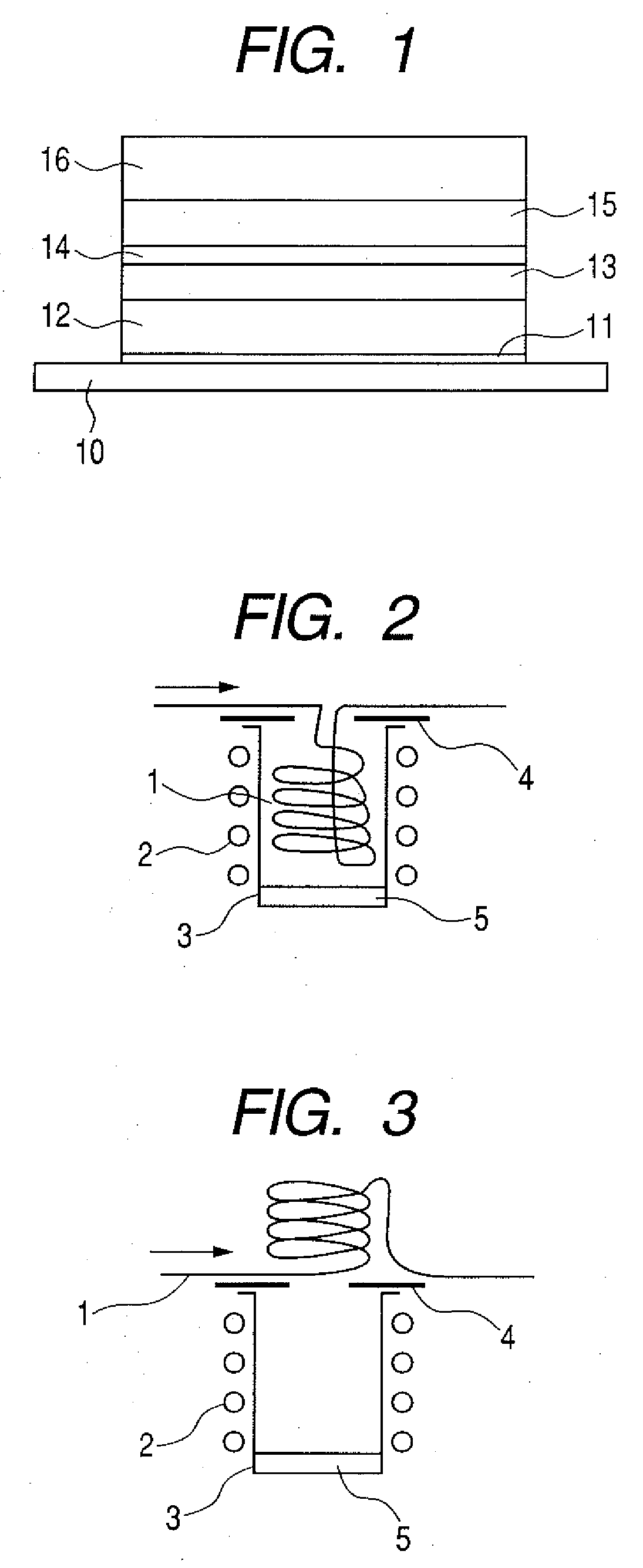
[0043] A device illustrated in FIG. 1 was manufactured. In this example, chromium (Cr) which functions as a reflecting electrode was used as the anode 11 and indium tin oxide (ITO) which functions as a transparent electrode for taking out emitted light was used as the cathode 16 to manufacture a top emission type device.

[0044] A chromium (Cr) film was formed on the substrate 10 by sputtering in a thickness of 200 nm to obtain the anode 11. After that, the substrate was cleaned with UV / ozone.

[0045] Then, the cleaned substrate and the material were loaded on a vacuum vapor deposition system (manufactured by ULVAC KIKO, Inc.). After exhausting air such that the pressure inside becomes 1×10⁻⁶ Torr, an N, N′-α-dinaphthylbenzidine (α-NPD) film was formed on the anode 11 in a thickness of 60 nm to form the hole transport layer 12. Further, a co-deposited film of coumarin 6 (1.0 wt %) and tris (8-hydroxyquinolinato) aluminum (Alq3) was formed thereon in a thickness of 30 nm to form the li...

example 2

[0054] As a vapor depositing source of cesium carbonate, one illustrated in FIG. 3 was used. More specifically, a tungsten filament as the medium 1 was provided above the alumina crucible 3, and vapor deposition was carried out with the tungsten filament heated by energization.

[0055] A device was manufactured by a method similar to that of Example 1 except for the above, and evaluation was made. The result is shown in Table 1.

example 3

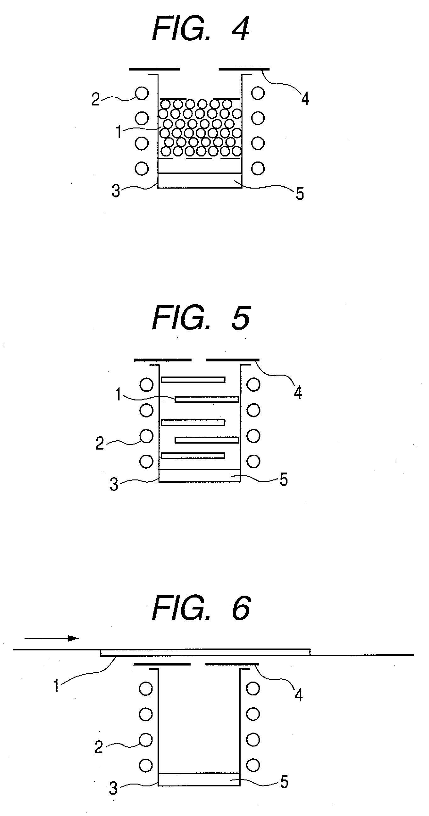
[0056] As a vapor depositing source of cesium carbonate, one illustrated in FIG. 4 was used. More specifically, spherical tungsten as the medium 1 was provided in the alumina crucible 3, and vapor deposition was carried out with the spherical tungsten indirectly heated by heat from the heat source 2. A thermocouple was attached to a bottom surface of the crucible 3 to measure the temperature, and the temperature was about 700° C.

[0057] A device was manufactured by a method similar to that of Example 1 except for the above, and evaluation was made. The result is shown in Table 1.

[0058] It is to be noted that, after vapor deposition of cesium carbonate was continuously carried out, the color of the spherical tungsten was changed to black, and the surface was covered with a residue. However, as shown in Table 1, although the initial value could not be maintained, it was confirmed that the characteristics could be continuously maintained.


PUM

PropertyMeasurementUnit
temperatureaaaaaaaaaa
vaporizing temperatureaaaaaaaaaa

Abstract

Provided is a method of manufacturing an organic light emitting device including the step of forming an electron injection layer. The step of forming the electron injection layer includes the steps of: vaporizing in a container a dopant material as a raw material of a dopant; causing the vaporized dopant material to pass a heated medium between the container and the substrate; and forming the organic compound into the electron injection layer. According to the method the organic light emitting device which has high electron injection efficiency and can be driven at a low voltage can be obtained.

Description

BACKGROUND OF THE INVENTION [0001] 1. Field of the Invention [0002] The present invention relates to a method of manufacturing an organic light emitting device and vapor deposition system. [0003] 2. Description of the Related Art [0004] An organic light emitting device is generally formed of a laminated structure including a substrate, an anode, a hole transport layer, a light emitting layer, an electron transport layer, an electron injection layer, and a cathode. In order to make lower the voltage of such an organic light emitting device, it is important to improve electron injectability from the cathode. More specifically, in order to improve electron injection efficiency, a metal, a metal compound, a metal salt, or the like having a low work function is used as a dopant. An organic layer containing such a dopant is used as the electron injection layer, and the dopant functions as a donor (electron donative) dopant. [0005] In an organic film of the electron injection layer, a meta...

Claims


Application Information

Patent Timeline
Patent Type & Authority Applications(United States)
IPC IPC(8): B05D5/06B05D5/12C23C16/00
CPCC23C14/24C23C14/243H01L51/001H01L51/002H01L51/5092H01L51/56H10K71/164H10K71/30H10K50/171H10K71/00
Inventor OTSUKA, MANABUTOKUNAGA, YUZOMASHIMO, SEIJIYOSHIKAWA, TOSHIAKIFUKUDA, NAOTO
Owner CANON KK
Why Eureka
Try Eureka