Cascaded mosfet embedded multi-input microcantilever

a multi-input, micro-cantilever technology, applied in the direction of mechanical measurement arrangement, mechanical roughness/irregularity measurement, instruments, etc., can solve the problems of insufficient performance of the array of currently available biosensors, time-consuming techniques, and large requirements for large-scale instruments

Inactive Publication Date: 2007-06-28
NORTHWESTERN UNIV
View PDF15 Cites 41 Cited by
  • Summary
  • Abstract
  • Description
  • Claims
  • Application Information

AI Technical Summary

Benefits of technology

[0009] More particularly, the sensor includes a structure and a field effect transistor embedded in the structure wherein the transistor has an associated electrical current that changes with mechanical perturbations in the structure.
[0010] In another embodiment of the present invention, the sensor includes a first structure with a first field effect transistor embedded therein, the first structure having a surface coated with a material to which a probe molecule will adhere. The sensor also includes a second structure used as a reference with a second field effect transistor embedded in the second, i.e. reference, structure. The first and second field effect transistors are coupled to a differential amplifier to provide an electrical signal indicative of mechanical perturbations in the first struc

Problems solved by technology

However, such techniques can be time consuming and often require relatively large, expensive instrumentation.
However, for most applications, arrays of currently available biosensors possess insufficient performance either due to large size, poor cross sensitivity, or long response times. Also, the majority of currently available biosensors are not compatible with complete CMOS Integration.
Either the operation parameters of the biosensor are incompatible with CMOS, e.g. radioactive or fluorescence labeling, or the biosensor materials cannot be integrated within a CMOS process.
However, the required optical system to measure cantilever deflection limits application to 10 s or 100 s of cantilevers and reduces its applicability to large (1000 s to 10,000 s) arrays.
Optical-based techniques also require a relati

Method used


Image

  • Cascaded mosfet embedded multi-input microcantilever
  • Cascaded mosfet embedded multi-input microcantilever
  • Cascaded mosfet embedded multi-input microcantilever

Examples


Embodiment Construction

[0056] The present invention relates to a novel sensor system based on silicon chip technology for electronic detection of molecular interactions. The present invention has ultra-high sensitivity, extremely low noise density and a cost effective technology platform and provides a powerful and easy to handle biological and chemical nanosensor for molecular and dangerous threat agent detection at ppb or ppq scale.

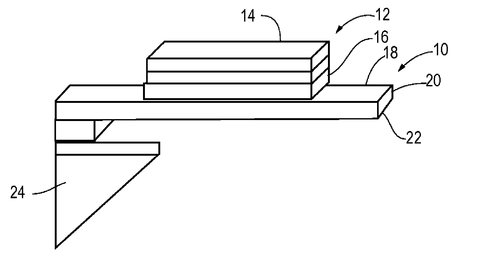
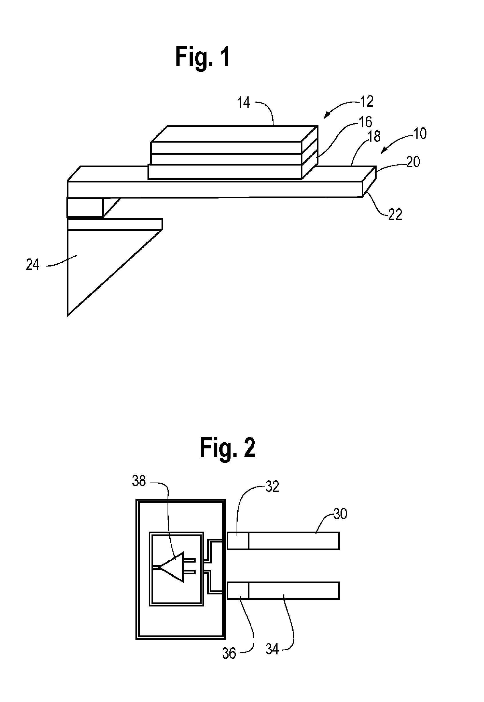
[0057] In accordance with one feature of the present invention, the sensing element is an integrated MOSFET (Metal Oxide Semiconductor Field Effect Transistor) transistor combined with a bipolar transistor, where the sensing element is placed at a high stress region of the microcantilever. The combined circuit of MOSFET and bipolar transistors is called BiMOS. The BiMOS platform not only has improved sensitivity, but also has an almost negligible noise figure (large signal to noise ratio), and ease of integration with CMOS and RF components. The micro-cantilever is immobiliz...


PUM


Abstract

A sensor for detecting mechanical perturbations represented by a change in an electrical signal includes a structure such as a cantilever, membrane, etc. and a field effect transistor such as a MOSFET embedded in the structure. The drain current of the embedded transistor changes with mechanical perturbations in the structure caused, for example, by a biochemical interaction being sensed. A scanning probe microscope utilizes the embedded MOSFET with a BiMOS actuator.

Description

CROSS-REFERENCE TO RELATED APPLICATIONS [0001] The present application claims the priority of provisional patent application Ser. No. 60 / 524,994 filed Nov. 11, 2003, and as a continuation-in-part of non-provisional application Ser. No. 10 / 996,274 filed Nov. 23, 2004, both of which are hereby incorporated herein by reference. STATEMENT REGARDING FEDERALLY SPONSORED RESEARCH OR DEVELOPMENT [0002] This work was supported by the National Science Foundation (NSF) awards: # NSEC-EEC-0118025, and ECS-0330410, and Air Force Office of Scientific Research (AFOSR)-MURI # F49620-00-1-0283.BACKGROUND OF THE INVENTION [0003] Most biosensors and chemical sensors rely on specific molecular recognition events. See for example, G. Miller, W. C. Inkret, M. E. Schillaci, H. F. Martz, T. T. Little, Health Physics, Volume 78 (2000) 598; N. Iznaga, G. Nunez, J. Solozabal, A. Morales, E. Artaza, R. Rubio, E. Cardenas, Computer Methods and Programs in Biomedicine, Volume 47 (1995) 167; W. Gopel, Chemical im...

Claims


Application Information

Patent Timeline
IPC IPC(8): G01N27/00
CPCG01N29/036G01N2291/0256G01N27/4145
Inventor SHEKHAWAT, GAJENDRADRAVID, VINAYAK P.
Owner NORTHWESTERN UNIV
Why Eureka
Try Eureka