Laser irradiation apparatus, laser irradiation method, and method for manufacturing semiconductor device

a laser irradiation and semiconductor technology, applied in the direction of manufacturing tools, instruments, optical elements, etc., can solve the problems of limited multimode optical fibers, difficult to directly use the above-described techniques, and large clad diameters of optical fibers, so as to improve the efficiency of laser irradiation treatment, and reduce the time for setting

Active Publication Date: 2007-07-05
SEMICON ENERGY LAB CO LTD
View PDF53 Cites 28 Cited by
  • Summary
  • Abstract
  • Description
  • Claims
  • Application Information

AI Technical Summary

Benefits of technology

[0032] By using the laser irradiation apparatus of the present invention, various effects can be obtained. Firstly, a laser beam can be propagated in a beam propagator while divergence of a beam diameter of the laser beam and short-term fluctuation of an optical axis are corrected by a transfer lens. Therefore, a laser beam emitted from the laser irradiation apparatus can be controlled without being hit on an inner wall of a pipe, whereby a semiconductor film can be irradiated while the energy is kept.
[0033] Secondly, by using the laser irradiation apparatus of the present invention, as long as a place to dispose a beam propagator is secured, even if a space is small, an object to be irradiated can be scanned with a laser beam. Therefore, irradiation with a laser beam, which is greater in quantity than a conventional one, can be performed at one time, whereby efficiency in laser irradiation treatment is significantly improved.
[0034] Thirdly, in the laser irradi

Problems solved by technology

Therefore, it is difficult to use the above-described technique directly.
The following is a problem in a case of using the first method.
Further, the optical fiber with a clad diameter which is so large that the optical fiber can withstand the above power density, is limited to a multimode optical fiber.
However, there is a problem in a condensing property because intensity distribution of the laser light which has passed through the multimode optical fiber becomes multimode.
If the clad diameter becomes small, a divergen

Method used


Image

  • Laser irradiation apparatus, laser irradiation method, and method for manufacturing semiconductor device
  • Laser irradiation apparatus, laser irradiation method, and method for manufacturing semiconductor device
  • Laser irradiation apparatus, laser irradiation method, and method for manufacturing semiconductor device

Examples


embodiment 1

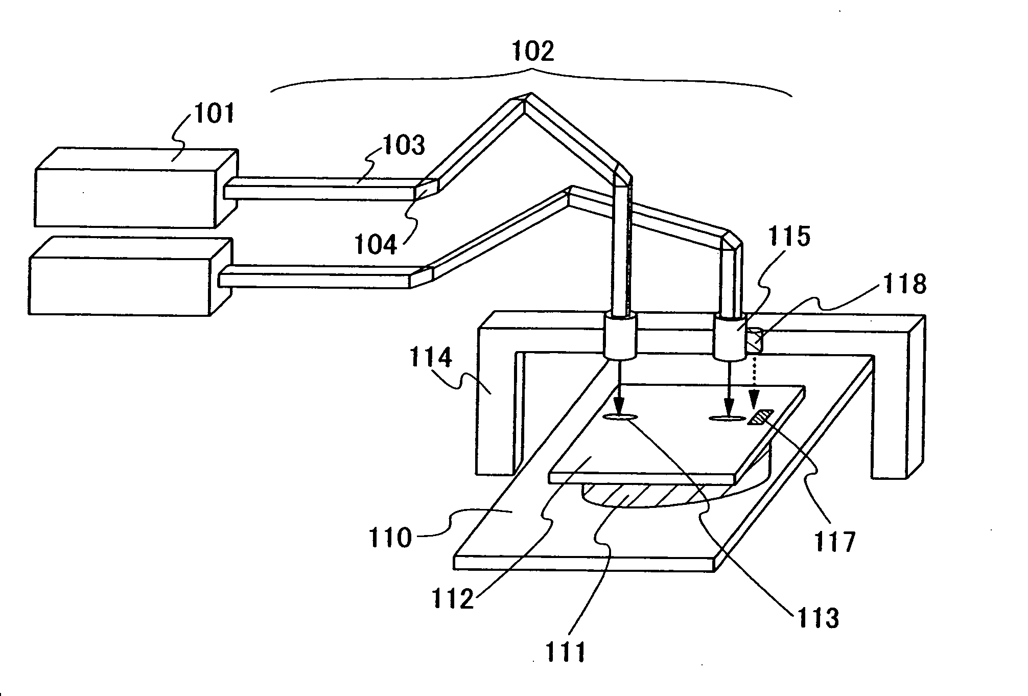
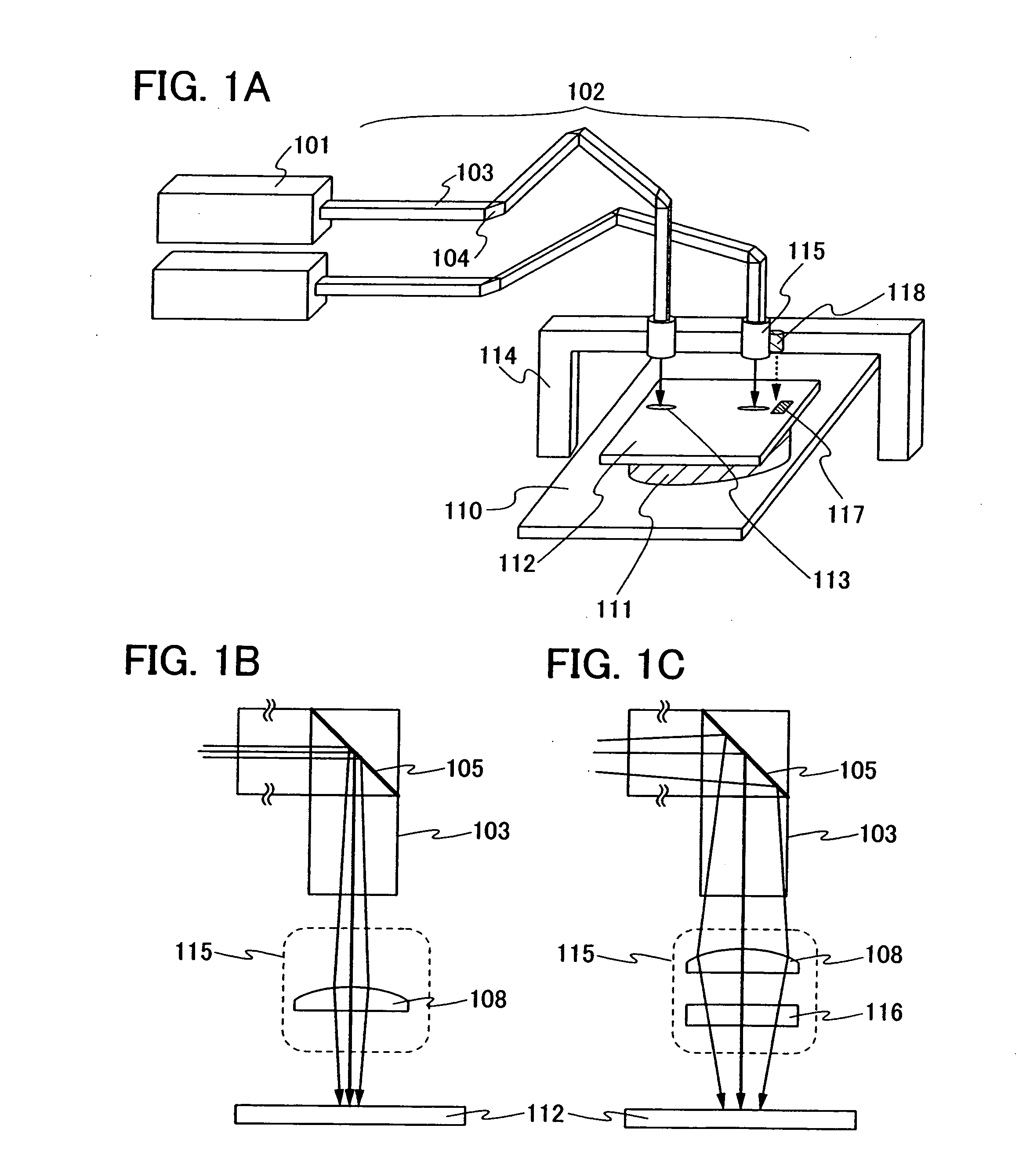
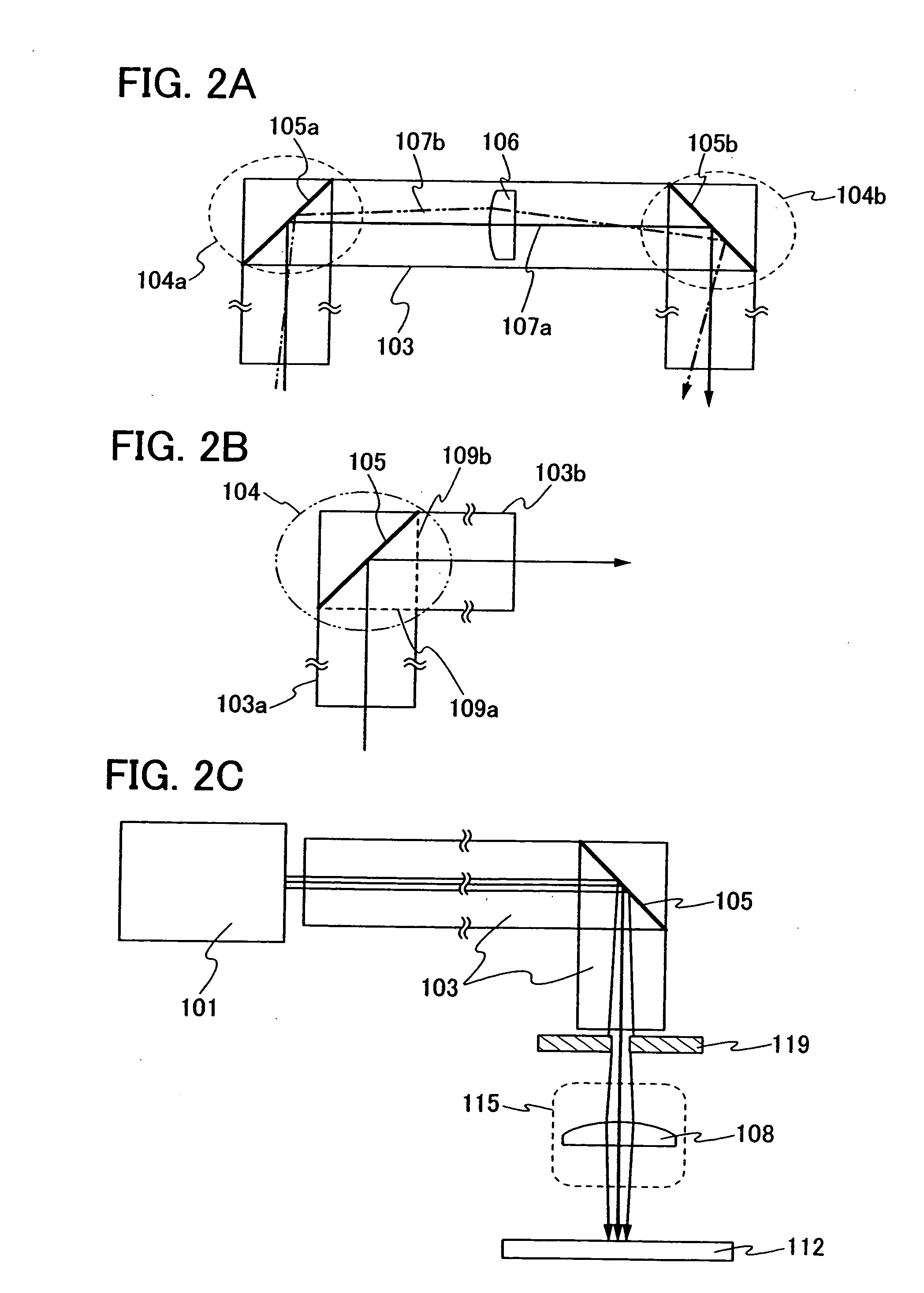
[0081] In this embodiment, an example of laser beam irradiation using a laser irradiation apparatus of the present invention will be explained. Although the embodiment mode shows an example in which a traveling direction of a laser beam is changed using a mirror in an articulated portion, this embodiment shows an example in which a traveling direction of a laser beam is changed using a prism.

[0082] As shown in FIG. 1A, an articulated beam propagator 102 included in the laser irradiation apparatus of the present invention is formed using pipes 103 connected by a rotatable articulated portion 104. A transfer lens 106 having an effect of suppressing change in beam profile is provided inside each pipe 103, and a prism is located in the articulated portion 104 by which the pipes 103 are connected to each other. The length of each pipe 103 can be freely set.

[0083] In this embodiment, a structure of an articulated portion which reflects a laser beam, which is different from the embodimen...

embodiment 2

[0110] In this embodiment, an example of a laser crystallization method, which is different from the above example, will be shown. In this embodiment, a laser in which ceramic YAG is doped with Yb is used for a laser oscillator. This laser has a wavelength in a near-infrared region and is capable of outputting power of 10 kW. This embodiment is not limited thereto, and a diode laser, an LD-pumped solid-state laser, or the like may be used. Although a CW laser is used in this embodiment, a pulsed laser having a repetition rate of greater than or equal to 10 MHz may also be used.

[0111] In a case of a laser crystal using the ceramic, a crystal larger than a single crystalline laser crystal can be easily formed; therefore, a longer oscillation light path can be obtained as compared with the case of using a single crystalline laser crystal. When the oscillation light path is long, amplitude is increased and a laser beam can be oscillated at high output. When a laser crystal with a paral...

embodiment 3

[0134] In this embodiment, an example of manufacturing a CMOS transistor using an n-channel TFT and a p-channel TFT manufactured using a laser irradiation apparatus of the present invention will be shown.

[0135]FIG. 5A shows a state which is immediately after performing laser irradiation using a plurality of laser irradiation apparatuses at the same time with respect to an amorphous semiconductor film 3002 formed over a substrate 3000 using the present invention. Hereinafter, a manufacturing process will be explained, which is viewed from a cross section taken along a dotted line A-B in FIG. 5A.

[0136] As shown in FIG. 5B, a base film 3001 is formed over the substrate 3000 having an insulating surface. In this embodiment, a glass substrate is used as the substrate 3000. As the substrate used here, a glass substrate made of barium borosilicate glass, alumino borosilicate glass, or the like; a quartz substrate; a ceramic substrate; a stainless steel substrate; or the like can be used....


PUM

PropertyMeasurementUnit
Degree of freedomaaaaaaaaaa

Abstract

A laser irradiation apparatus is provided with a laser oscillator, an articulated beam propagator in which a plurality of pipes are connected to each other in an articulated portion, and a course change means of a laser beam in the articulated portion. At least one pipe of the plurality of pipes includes a transfer lens for suppressing stagger of a laser beam in a traveling direction, in each pipe. The articulated portion produces degree of freedom in disposition of a laser oscillator, and the transfer lens enables suppression of change in beam profile.

Description

TECHNICAL FIELD [0001] The present invention relates to a laser irradiation apparatus for processing an object to be irradiated by irradiation with a laser beam, which is introduced to the object to be irradiated. Specifically, the present invention relates to a laser irradiation apparatus for uniformly and efficiently performing annealing on a semiconductor material or the like; a laser irradiation method using the laser irradiation apparatus; and a semiconductor device manufactured using the laser irradiation apparatus and the laser irradiation method, and a method for manufacturing the semiconductor device. BACKGROUND ART [0002] In recent years, a technique of manufacturing a thin film transistor (hereinafter, referred to as a TFT) over a substrate has been drastically progressing, and the application and development thereof to an active matrix display device, a thin film integrated circuit device, and the like has been advanced. In particular, a TFT using a polycrystalline semic...

Claims


Application Information

Patent Timeline
IPC IPC(8): B23K26/04H01L21/20
CPCB23K26/06H01L27/1292B23K26/0639B23K26/0643B23K26/0652B23K26/0665B23K26/0823B23K26/0838B23K26/0869B23K26/0892B23K26/1452B23K26/38B23K26/4075B23K2201/40H01L21/2026H01L27/1266H01L29/42384H01L29/4908H01L27/1285B23K26/0635B23K2101/40B23K2103/50B23K26/064B23K26/0624B23K26/1438B23K26/40H01L21/0242H01L21/02683H01L21/02691H01L21/02381H01L21/02505H01L21/02529H01L21/02502H01L21/02532H01L21/02686H01L21/02425H01L21/02488H01L21/02422H01L21/02672H01L21/02678H01L21/02675
Inventor TANAKA, KOICHIROYAMAMOTO, YOSHIAKI
Owner SEMICON ENERGY LAB CO LTD
Why Eureka
Try Eureka