Semiconductor device and method of manufacturing the same

a technology of semiconductor devices and semiconductors, applied in the field of semiconductor devices, can solve the problems of low production scale, low throughput, and inability to become commercially practical, and achieve the effect of improving the performance of semiconductor devices

Inactive Publication Date: 2007-07-12
NEC CORP
View PDF5 Cites 26 Cited by
  • Summary
  • Abstract
  • Description
  • Claims
  • Application Information

AI Technical Summary

Benefits of technology

[0030] In addition, the present invention provides a system of improving the performance of a semiconductor device having a nanowire.

Problems solved by technology

The lower limit of the production scale according to this technique, however, is about several tens of nanometers.
This process, however, has not become commercially practical, because it achieves only a low throughput.
Silicon is a representative semiconductor material but will reach its limitations as a material soon.
Current bottom-up micromachining techniques, however, are still susceptible to improvements in industrial applications.
This is because these techniques are difficult to “constitute a desired structure in a desired place”, and techniques of “constituting a desired structure in a desired place” have not been provided yet.
These manufacturing techniques confuse natural order of things.
It does not provide a semiconductor device operating at high speed and consuming less electric power.
In addition, it does not establish a technique of manufacturing the semiconductor device.
The above-mentioned techniques also include problems from the viewpoint of materials.
These techniques do not theoretically satisfy requirements on on-state current in next-generation transistors, as long as they use the above-mentioned materials as channels.
In addition, these materials including organic molecules or nanoparticles have a more serious problem.
Consequently, the resulting devices are impossible to operate at high speed, and the higher-performance of semiconductor devices may not be achieved,
However, semiconductor devices having smaller dimensions may not be achieved by the conventional processing techniques using lithography and etching, even if such good materials are used.
These techniques are disadvantageous in the methods of manufacturing the transistors.
The advantages of carbon nanotubes as a material are not fully enjoyed, and the next-generation semiconductor devices having smaller dimensions are not provided, as long as the top-down micromachining techniques are used.
The growth of coaxial hetero nanowires according to these techniques, however, is not a so-called “in situ growth”.
Accordingly, semiconductor devices having smaller dimensions are not provided by the techniques having these disadvantages.
The techniques are insufficient as manufacturing techniques in industrial applications.

Method used


Image

  • Semiconductor device and method of manufacturing the same
  • Semiconductor device and method of manufacturing the same
  • Semiconductor device and method of manufacturing the same

Examples


first embodiment

[0062]FIGS. 6A, 6B, 6C, 6D, 6E, and 6F show a method of manufacturing a field-effect transistor according to First Embodiment. These figures also show the resulting field-effect transistor.

[0063] Initially, a single-layer carbon nanotube 50 was placed in a vacuum system. Electric power was supplied to the carbon nanotube 50 from a power supply 5 through an interconnection 6 (FIG. 6A). Consequently, the carbon nanotube 50 was self-heated by the action of Joule heat according to the supplied power. It emitted heat, light, and thermoelectrons to a minute region in the vicinity of the carbon nanotube 50. Next, a raw material 51 including oxygen (O2) and silane (SiH4) was supplied into the vacuum system so as to form a silicon oxide layer 52 as a gate insulating layer. The heat, light, and thermoelectrons formed as a result of self-heating acted as an energy source. They caused the thermal decomposition of the raw material 51. They also caused the solid phase growth of decomposed produc...

second embodiment

[0069]FIGS. 7A, 7B, 7C, and 7D are schematic diagrams showing the procedures of manufacturing a ring oscillation circuit according to Second Embodiment of the present invention. The ring oscillation circuit comprises inverters in combination. Each of the inverters comprises a p-type carbon nanotube field-effect transistor and an n-type carbon nanotube field-effect transistor.

[0070] In this embodiment, the external energy for processing is an electromagnetic wave resonating energy levels of the carbon nanotube. Initially, undoped intrinsic semiconductor carbon nanotubes 50 were prepared, and an electromagnetic wave was applied to regions 55 in FIG. 7A while feeding a raw material of a p-type dopant (FIG. 7A). Consequently, p-type carbon nanotubes 56 were formed (FIG. 7B). Next, an electromagnetic wave was applied to regions 55 in FIG. 7B while feeding a raw material of an n-type dopant. Consequently, n-type carbon nanotubes 57 were formed (FIG. 7C). Finally, a source-electrode leadi...

third embodiment

[0071]FIG. 8 shows the drain current-gate voltage characteristic of a carbon nanotube field-effect transistor. The field-effect transistor shows conduction converted from p-type conduction to ambipolar conduction by the method according to an embodiment of the present invention.

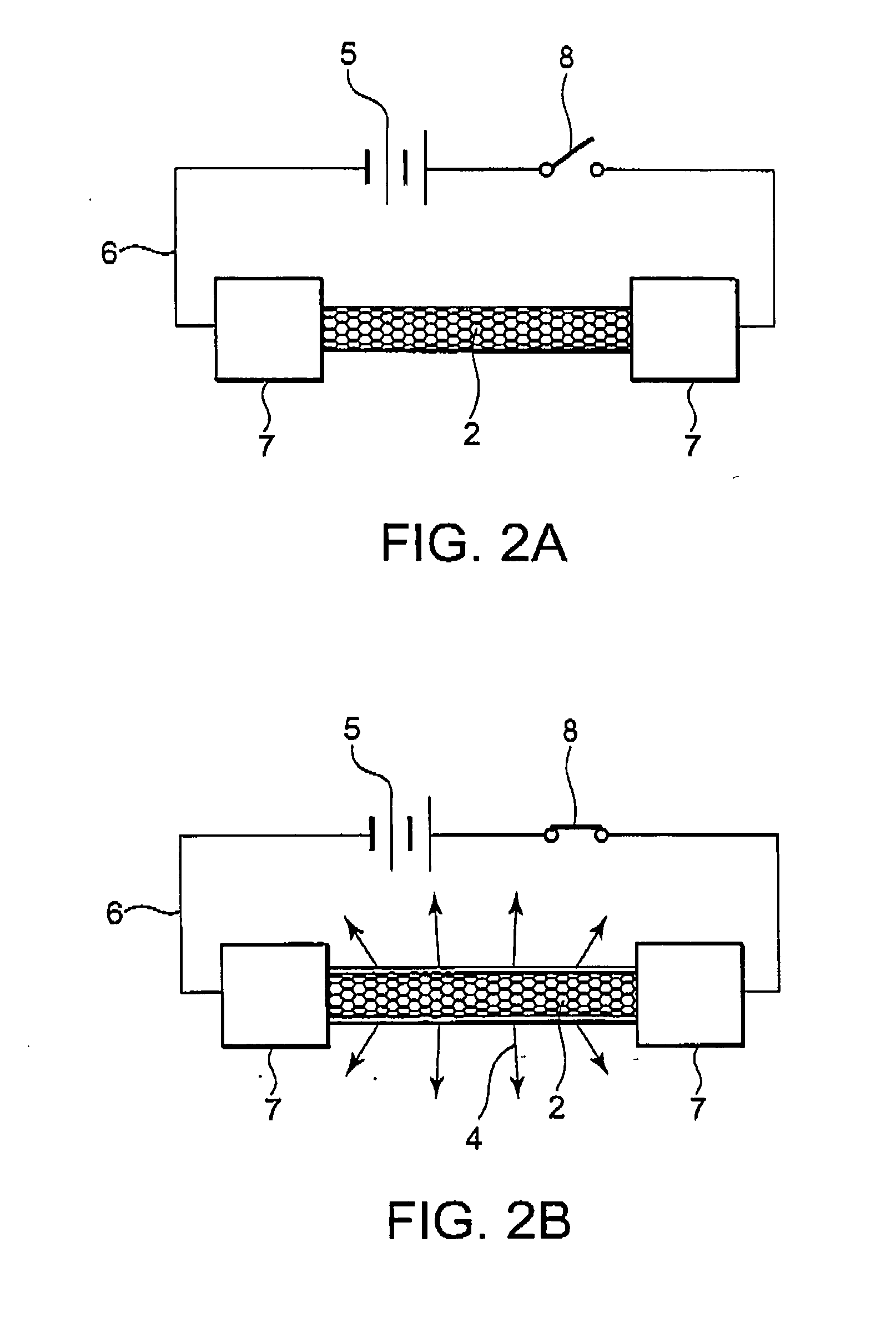
[0072] In this embodiment, electric power was applied as the external energy. The electric properties of the field-effect transistor were determined using the measuring system in FIG. 5. The drain voltage in these measurements was set at 10 mV. The characteristic curve (a) in FIG. 8 shows the drain current-gate voltage characteristic of the field-effect transistor before power supply. The characteristic curves (b), (c), and (d) show the drain current-gate voltage characteristics after electric power of 180 μW, 380 μW, and 920 μW were supplied, respectively. The characteristic curve (a) demonstrates that the carbon nanotube field-effect transistor shows p-type conduction in which the drain current increases a...


PUM

PropertyMeasurementUnit
diameteraaaaaaaaaa
temperatureaaaaaaaaaa
ionization potentialaaaaaaaaaa

Abstract

A self-aligned / self-limited processing is carried out on a nanowire material typified by a carbon nanotube or on the vicinity of the nanowire material alone in the following manner. External energy is applied to the nanowire material. Joule heat, light, or a thermoelectron is thereby locally formed and acts as minute energy. The minute energy causes a chemical reaction of an externally added raw material and causes the conversion of a property of the nanowire material.

Description

[0001] This application claims priority to prior Japanese patent application JP 2005-315627, the disclosure of which is incorporated herein by reference. BACKGROUND OF THE INVENTION [0002] 1. Field of the Invention [0003] The present invention relates to semiconductor devices and methods of manufacturing the same. More specifically, it relates to semiconductor devices constitutionally containing semiconductor materials having a nanowire structure, typified by carbon nanotubes. It also relates to methods of manufacturing the semiconductor devices. [0004] 2. Description of the Related Art [0005] Following advancing information communication technologies, demands have been made on semiconductor devices that can operate at high speed and consume less electric power, and on techniques for manufacturing such semiconductor devices. Recent semiconductor devices basically include metal oxide semiconductor (MOS) elements using silicon as a semiconductor material. These MOS elements have been ...

Claims


Application Information

Patent Timeline
Patent Type & Authority Applications(United States)
IPC IPC(8): H01L21/20H01L21/36
CPCB82Y10/00H01L51/0512H01L51/0048H10K85/221H10K10/462
Inventor HIURA, HIDEFUMITADA, TETSUYAKANAYAMA, TOSHIHIKO
Owner NEC CORP
Why Eureka
Try Eureka