Method of recycling wasted printed-circuit-board

a technology of printed circuit board and waste, which is applied in the direction of climate sustainability, electric cable installation, final product manufacturing, etc., can solve the problems of not only impurity effect, but also certain difficulty in recycling disposal, and the recycling value of brominated epoxy resin and fiberglass after collection is neglected, and consumes a lot of energy

Inactive Publication Date: 2007-07-26
WU HSIEH SEN
View PDF7 Cites 24 Cited by
  • Summary
  • Abstract
  • Description
  • Claims
  • Application Information

AI Technical Summary

Benefits of technology

[0022]In other words, the present invention takes advantage of the characteristics of the PCB so as to dispose different recycling material in stage manner, so that different metals remaining on said PCB are sorted out step by step; Thereby, the bromide and the fiberglass of importance in the resins are collected and converted into variety of industrial materials as resource for recycling in order to prevent said wasted PCB from spoiling the natural environment after recycling.

Problems solved by technology

First pulverize the wasted PCBs into powder, then sort said powder into two categories of more metallic powder and less metallic powder; Regardless of what kind of powder aforesaid, the ingredients contain mixture of brominated epoxy resins and fiberglass in addition of the metal so that causing not only impurity effect but also certain difficulty in recycling disposal; Especially, both of the recycling value of said brominated epoxy resins and fiberglass after collecting are neglected.
Directly incinerate and melt the wasted PCBs into mixture of fiberglass and metal, then extract the essential metals after cooling; The process not only consumes much energy but also creates environmental pollution issue owing to the toxic hydrogen bromide [BrH] byproduct; Besides, the collected materials, which are low-grade mixture of metal, must re-smelt to purify for recycling use so that the value of direct utilization is very low.
A tremendous amount toxic hydrogen bromide [BrH] gas is produced during heating decomposition process so that seriously jeopardizing natural environment; Excepting the metal being recyclable by sorting, the rest materials such as brominated epoxy resins and fiberglass are not recyclable with potentiality of spoiling environment.
a. Upon processing temperature over 400° C., the tin, lead and copper in said wasted PCBs will mix into alloy such that becoming low-grade metal mixture, which not only incurring extra cost expense but also wasting time and effort for refinement.
b. The wasted PCBs will float on the melted inorganic salt as the specific weight of the melted inorganic salt is greater than that of the wasted PCBs; Thereby, the agitating separation process is difficult to directly operate.
c. The agitating shattering process will fail as the wasted PCBs softening with flexibility after the dissolution of the melted inorganic salt.
The finished PCBs are interconnected by electroplating joint with soldering point being bigger than through-hole such that fiberglass of PCBs being tightly bonded; Thereby, the effect in separating process of fiberglass is relative low due to difficulty.
The fiberglass will be ruined as the wasted PCBs being put in the melted inorganic salt over a long period of time; The collecting of said fiberglass is difficult as operating time in the mix-agitating process and the re-extracting process is uncontrollable and inconsistent;
Accordingly, all the conventional methods aforesaid in disposing wasted PCB are not the ideal perfect disposal method.

Method used


Image

  • Method of recycling wasted printed-circuit-board
  • Method of recycling wasted printed-circuit-board
  • Method of recycling wasted printed-circuit-board

Examples


Embodiment Construction

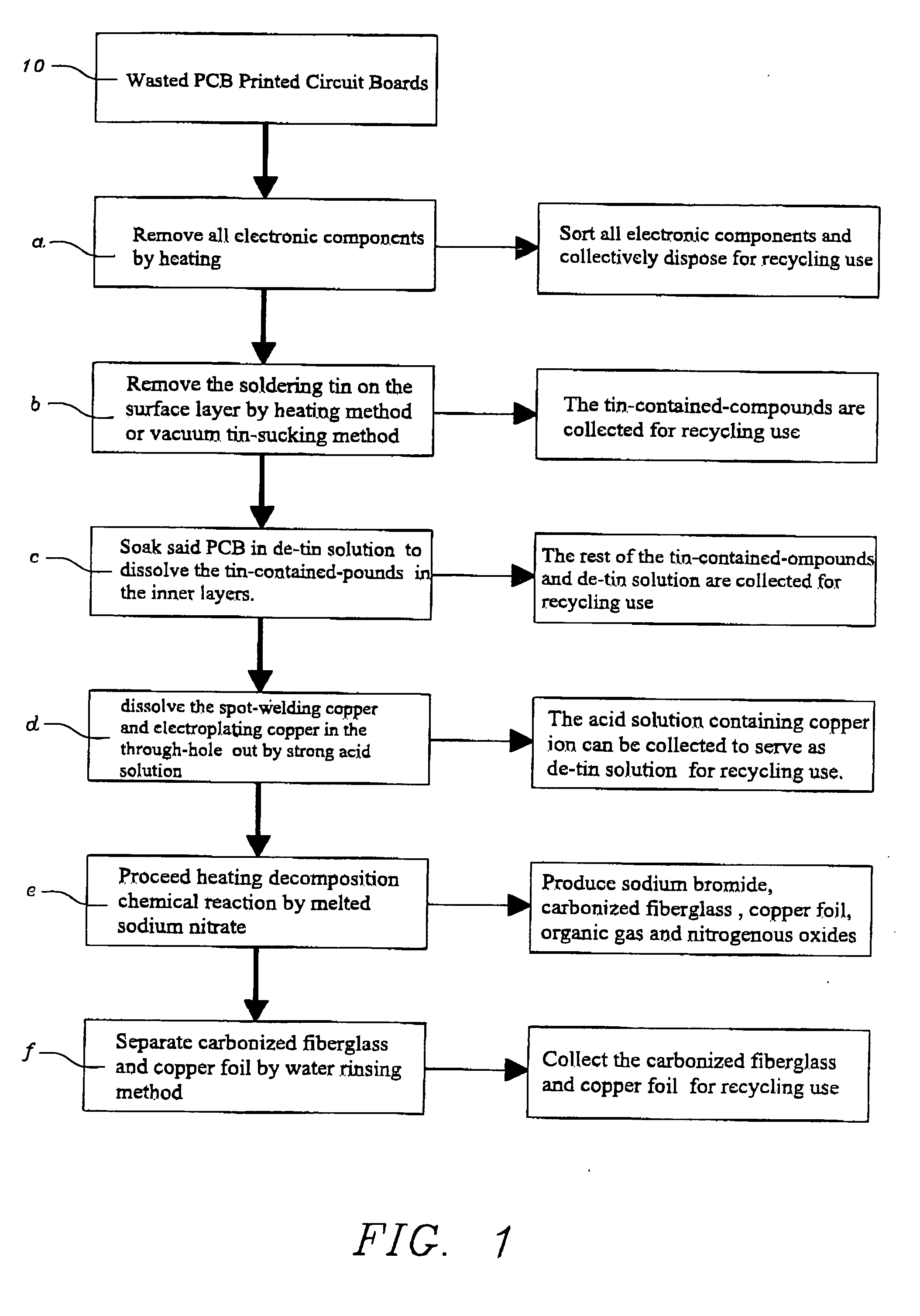
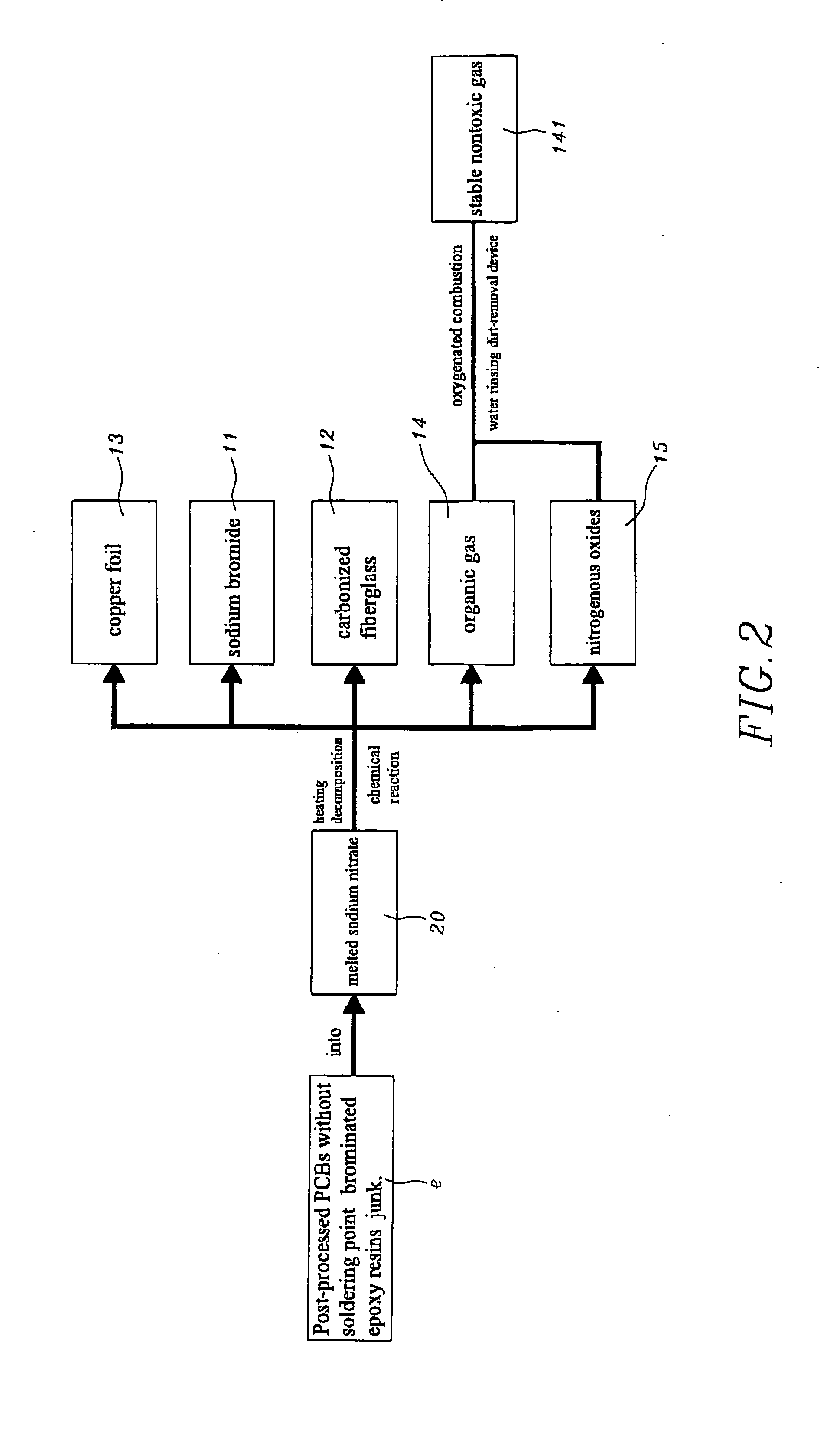
[0026]As shown in the figures of number 1 and 2, the present invention is a method of recycling wasted printed-circuit-board with disposal steps comprising:

[0027]a. Remove all electronic components on all wasted PCBs 10 by heating them on their soldering points such that becoming wasted PCBs without any electronic component then collectively sort and dispose them for recycling use.

[0028]Heat all such wasted PCBs without any electronic component over to 200° C. to melt soldering tin on their surface layer so as to remove and collect the tin-contained-compounds, whose melting point being 200° C.; then directly collect them by vacuum tin-sucking method for recycling use.

[0029]c. Soak said wasted PCBs at step b in de-tin solution of market finished product to dissolve the tin-contained-compounds in the inner layers to separate it from copper; then directly collect all of tin-contained-compounds by said de-tin solution for recycling use.

[0030]d. Apply strong acid solution on said wasted ...


PUM

PropertyMeasurementUnit
temperatureaaaaaaaaaa
melting pointaaaaaaaaaa

Abstract

The present invention relates to a “method of recycling wasted printed-circuit-board”, which takes advantage of the characteristics of the PCB so as to dispose different recycling material in stage manner, so that different metals remaining on said PCB are sorted out step by step; Thereby, the bromide and the fiberglass of importance in the resins are collected and converted into variety of industrial materials as resource for recycling use in order to prevent said wasted PCB from spoiling the natural environment after recycling use.

Description

FIELD OF THE PRESENT INVENTION[0001]The present invention relates to the method of recycling wasted printed-circuit-board, particularly for the method and equipment thereof in collecting the different metals remaining on the recyclable wasted PCB being converted into recycling industrial materials under the standard of avoiding second pollution.BACKGROUND OF THE INVENTION[0002]As everyone knows, the PCB has been largely used in variety of electric products; Worryingly, the heavy metals in the wasted PCBs such as tin, lead and copper etc. can easily cause second social effects of pollution if those wasted PCBs did not collected for recycling or disposed unsuitably when they are discarded as junk; Especially, the brominated epoxy resins of halide in said wasted PCBs are much easier to spoil natural environment; that is why all the environmental protection experts of every country in the world without exception strive for advocating in reducing the utility rate of using halide material...

Claims


Application Information

Patent Timeline
Patent Type & Authority Applications(United States)
IPC IPC(8): H01B15/00
CPCB29B17/02Y10T29/49755B29B2017/0255B29B2017/0293B29B2017/0496B29K2063/00B29K2105/06B29K2105/065B29K2705/00B29K2705/10B29L2031/3425C22B7/001C22B7/005H05K3/067H05K3/22H05K3/3494H05K2203/0361H05K2203/176H05K2203/178B29B17/04Y02P10/20Y02P70/50Y02W30/62Y02W30/50Y02W30/82B09B3/29
Inventor WU, HSIEH SEN
Owner WU HSIEH SEN
Why Eureka
Try Eureka