Semiconductor memory

a technology of semiconductors and memory, applied in the field of semiconductor memory, can solve the problems of high-speed memory, low access speed, unsuitable for forming large-capacity memory, etc., and achieve the effects of increasing the critical delamination load, enhancing the adhesive strength of chalcogenide materials, and increasing the delamination strength

Inactive Publication Date: 2007-07-26
RENESAS ELECTRONICS CORP
View PDF14 Cites 36 Cited by
  • Summary
  • Abstract
  • Description
  • Claims
  • Application Information

AI Technical Summary

Benefits of technology

[0018] The major effects of the present invention will now be briefly described.
[0019] The adhesive layers formed over and under the chalcogenide material layer can prevent delamination of the chalcogenide material layer during the manufacturing process. Further, the protective film formed on the sidewalls of the chalcogenide material layer can prevent sublimation of the chalcogenide material layer during the manufacturing process.
[0020] A first means of the present invention is to form adhesive layers over and under the chalcogenide material (layer) so as to enhance the adhesive strength of the chalcogenide material (at its interfaces with the overlying and underlying layers).
[0021] First, the effects of these adhesive layers will be described. We formed GeSbTe films on SiO2 films to a thickness of 100 nm, and performed a scratch test on these GeSbTe films to compare their delamination strength. In a scratch test, a thin film surface of a sample is scratched by an indenter while applying a load to the sample in the vertical direction, in order to determine the minimum load that cause delamination (referred to as the “critical delamination load”). The higher the critical delamination load, the higher the delamination strength. FIG. 8 shows the (critical delamination load) measurement results. As shown in FIG. 8, the delamination strength of the GeSbTe film was extremely low when an adhesive layer was not inserted (between the GeSbTe film and the SiO2 film). Further, insertion of a W layer did not lead

Problems solved by technology

A DRAM provides large capacity but its access speed is low.
A SRAM, on the other hand, is high-speed memory, but is not suitable for forming a large capacity memory, since each cell requires a number of transistors (4 to 6 transistors) and hence it is difficult to produce highly integrated SRAM.
However, the flash memory i

Method used


Image

  • Semiconductor memory
  • Semiconductor memory
  • Semiconductor memory

Examples


first embodiment

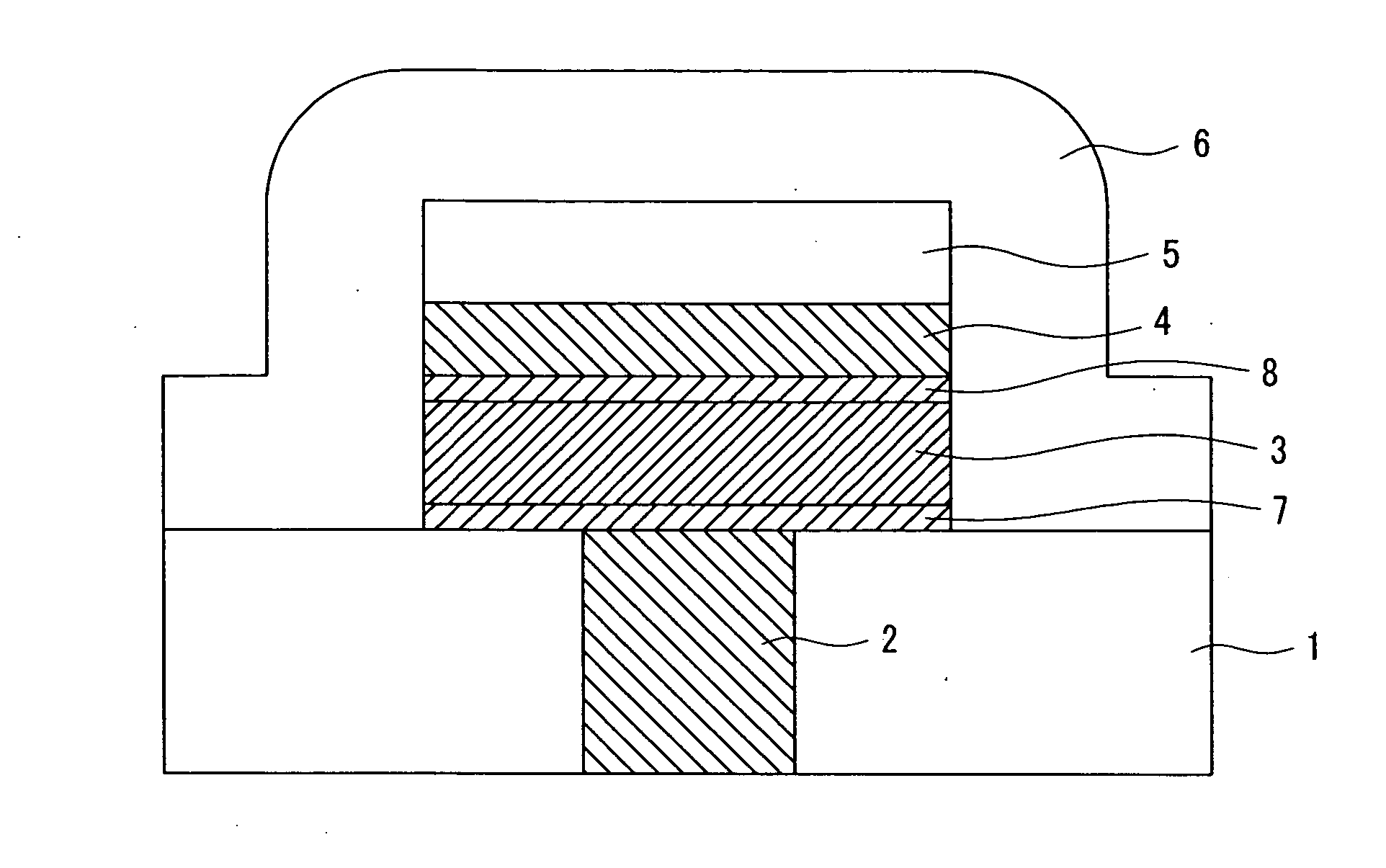
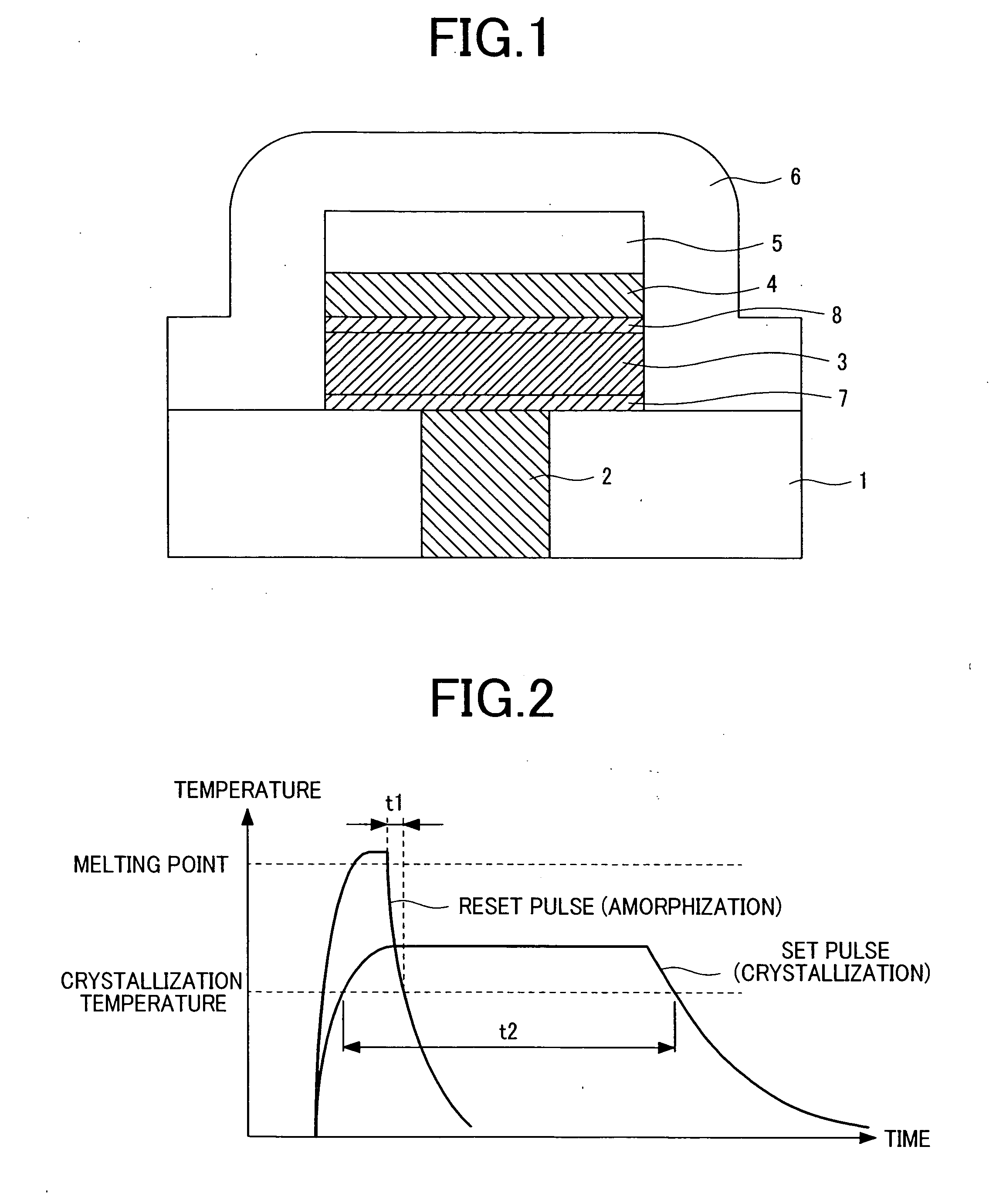
[0039] A first embodiment of the present invention will be described with reference to FIG. 12. This embodiment provides an example in which conductive adhesive layers are formed both over and under the chalcogenide material layer.

[0040] First of all, a semiconductor substrate 101 is provided, and a MOS transistor is formed on the substrate as a select transistor. Specifically, trench isolation (or device separation) oxide films 102 for isolating the MOS transistor are formed in the surface of the semiconductor substrate 101 by a known selective oxidation technique or shallow trench isolation technique. The present embodiment uses the shallow trench isolation technique, which also can planarize the surface. First, isolation trenches are formed in the substrate by a known dry etching technique. Then, after removing damage left on the sidewalls and bottoms of the trenches in the previous dry etching process, an oxide film is deposited by a known CVD technique. Then, portions of the o...

second embodiment

[0054] A second embodiment of the present invention will be described with reference to FIG. 13. This embodiment provides an example in which: a conductive adhesive layer is formed at the interface between the chalcogenide material layer and the plug; an insulative adhesive layer is formed at the interface between the chalcogenide material layer and the interlayer insulating film; and a conductive adhesive layer is formed at the interface between the chalcogenide material layer and the upper electrode.

[0055] Since the steps before and including the step of forming the tungsten plug 112 are the same as those described in connection with the first embodiment, a description of these steps is not provided herein.

[0056] There will now be described a process of forming an insulative adhesive layer 121 and a conductive adhesive layer 122 on the interlayer insulating film 111 and on the tungsten plug 112, respectively, in a self-aligned manner. First, a titanium layer is deposited on the ...

third embodiment

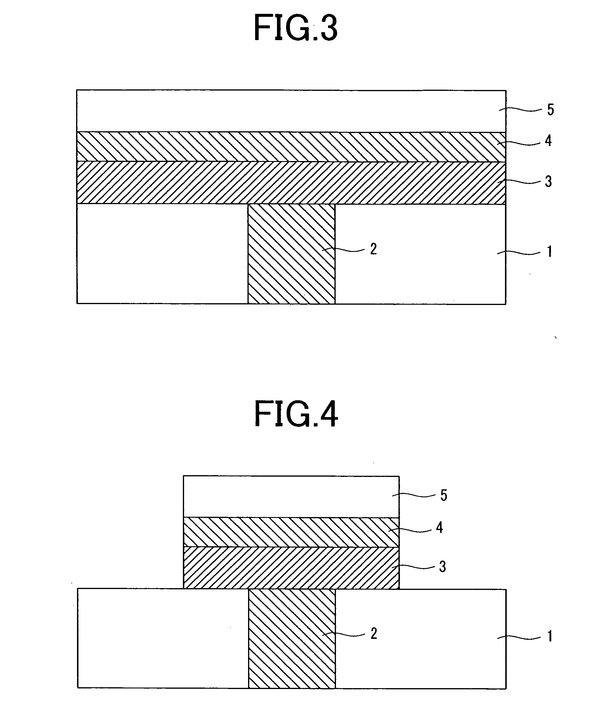
[0064] A third embodiment of the present invention will be described with reference to FIG. 14. This embodiment provides an example in which a protective film is formed on the sidewalls of the chalcogenide material layer. Since the steps before and including the step of forming the tungsten plug 112 are the same as those described in connection with the first embodiment, a description of these steps is not provided herein.

[0065] First, a chalcogenide material layer 114 of GeSbTe having a thickness of 100 nm and an upper electrode 116 of tungsten having a thickness of 50 nm are sequentially deposited over the entire surfaces of the interlayer insulating film 111 and the tungsten plug 112 by a known sputtering technique. After that, a silicon oxide film 117 is deposited by a known CVD technique. Then, the silicon oxide film 117, the upper electrode 116, and the chalcogenide material layer 114 are sequentially processed by a known lithographic process and dry etching process. It shoul...


PUM


Abstract

Manufacturing processes for phase change memory have suffered from the problem of chalcogenide material being susceptible to delamination, since this material exhibits low adhesion to high melting point metals and silicon oxide films. Furthermore, chalcogenide material has low thermal stability and hence tends to sublime during the manufacturing process of phase change memory. According to the present invention, conductive or insulative adhesive layers are formed over and under the chalcogenide material layer to enhance its delamination strength. Further, a protective film made up of a nitride film is formed on the sidewalls of the chalcogenide material layer to prevent sublimation of the chalcogenide material layer.

Description

TECHNICAL FIELD [0001] The present invention relates to a technique that is effective when applied to semiconductor integrated circuit devices which employ phase change memory cells formed of a phase change material such as chalcogenide. BACKGROUND ART [0002] Mobile devices, typified by cellular phones, use a semiconductor memory such as a DRAM, SRAM, or flash memory. A DRAM provides large capacity but its access speed is low. A SRAM, on the other hand, is high-speed memory, but is not suitable for forming a large capacity memory, since each cell requires a number of transistors (4 to 6 transistors) and hence it is difficult to produce highly integrated SRAM. DRAM and SRAM must continuously receive power to retain data; that is, they are volatile memories. Flash memory, on the other hand, is a nonvolatile memory; it does not need to continuously receive power to electrically retain data. However, the flash memory is disadvantageous in that its program / erase count is limited to a max...

Claims


Application Information

Patent Timeline
IPC IPC(8): H01L29/04H01L27/10H01L27/24H01L45/00
CPCH01L45/06H01L45/12H01L45/1233H01L27/2436H01L45/144H01L45/1675H01L45/126H10B63/30H10N70/801H10N70/231H10N70/8413H10N70/826H10N70/8828H10N70/063H10N70/8825H10N70/841
Inventor MATSUI, YUICHIMATSUZAKI, NOZOMUTAKAURA, NORIKATSUYAMAMOTO, NAOKIMATSUOKA, HIDEYUKIIWASAKI, TOMIO
Owner RENESAS ELECTRONICS CORP
Why Eureka
Try Eureka