Mold for imprint, process for producing minute structure using the mold, and process for producing the mold
a technology of imprint and mold, which is applied in the direction of photomechanical equipment, applications, instruments, etc., can solve the problems of large amount of mold preparation time and cost, difficult to prepare seamless patterns having a larger area than the mold at the substrate surface, and long and complicated photolithographic process. , to achieve the effect of reducing or no seam area
- Summary
- Abstract
- Description
- Claims
- Application Information
AI Technical Summary
Benefits of technology
Problems solved by technology
Method used
Image
Examples
embodiment 1
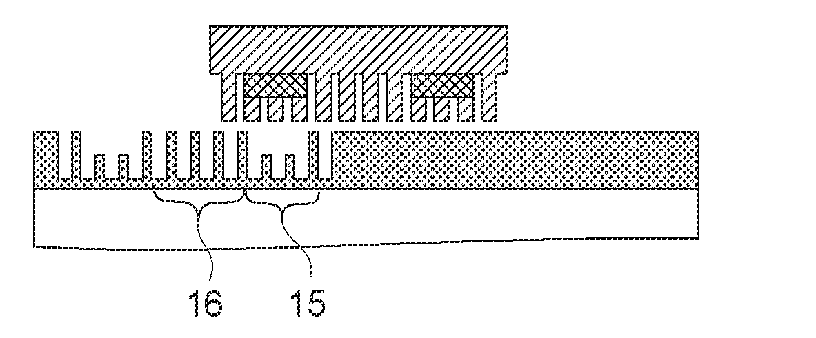
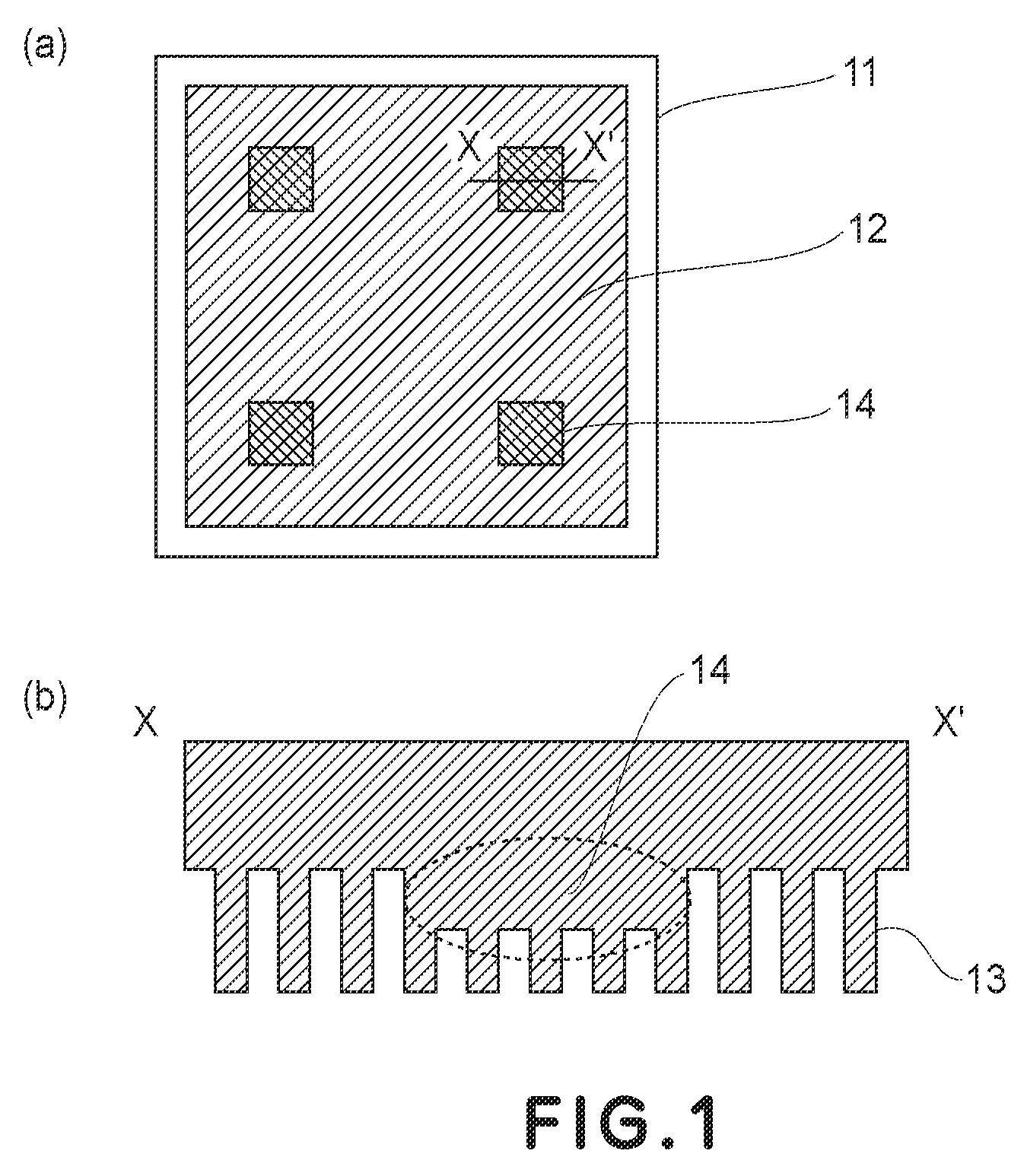
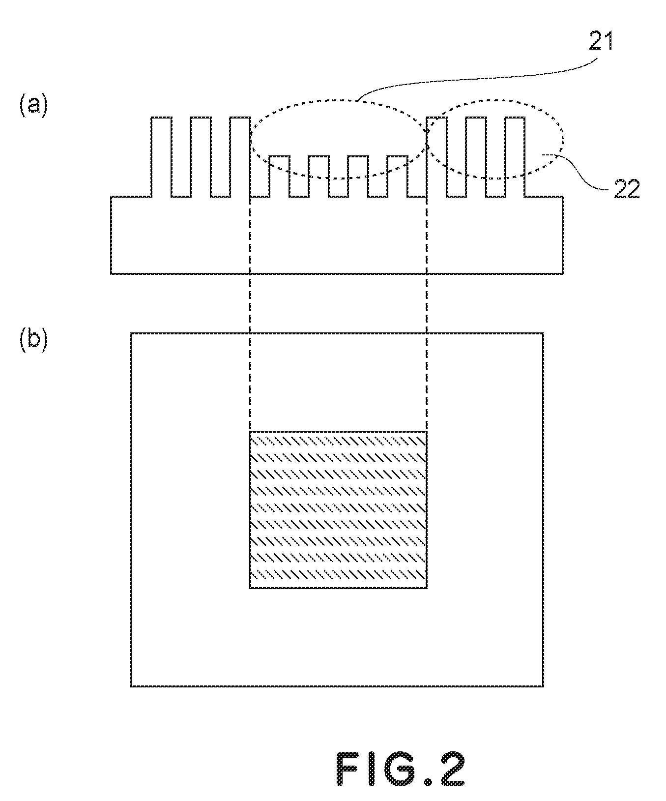
[0119]In Embodiment 1, a production process of a quartz-mode mold for nanoimprint having an optically recognizable sub-pattern and a production process of a nanostructure using the mold according to the present invention will be described.
[0120]In this embodiment, as a substrate for preparing a mold, a 1.2 mm-thick quartz substrate having a 10 mm square area is used.
[0121]At the surface of the quartz substrate, a 20 nm-thick layer (film) of Al is formed by sputtering and thereon, a 30 nm-thick resist for electron beam lithography is formed by spin coating.
[0122]In a 5 mm square area, a pattern including a constant-pitch slit pattern having a pitch of 200 nm and a width of 100 nm is formed by light exposure and development.
[0123]Thereafter, by dry etching, a thin line pattern having a pitch of 200 nm and a width of 100 nm is formed in the Al layer.
[0124]Then, by using the Al layers an etching mask, a recess structure having a pitch of 200 nm, a line width of 100 nm, and a depth of 30...
embodiment 2
[0135]In Embodiment 2, a production process of a quartz-mode mold for nanoimprint having a constitution different from that in Embodiment 1 and a production process of a nanostructure using the mold according to the present invention will be described.
[0136]In this embodiment, as a substrate for preparing a mold, 1.2 mm-thick quartz substrate having a 10 mm square is used.
[0137]At the surface of the quartz substrate, a 20 nm-thick layer (film) of Al is formed by sputtering and thereon, a 30 nm-thick resist for electron beam lithography is formed by spin coating.
[0138]In a 5 mm square area, a pattern including a constant-pitch circular clear portion pattern having a pitch of 160 nm and a diameter of 80 nm is formed by light exposure and development.
[0139]Thereafter, by dry etching, circular clear portions having a pitch of 160 nm and a diameter of 80 nm are formed in the Al layer.
[0140]Then, by using the Al layers an etching mask, a recess structure having a pitch of 160 nm, a diamet...
embodiment 3
[0157]In Embodiment 3 a production process of a quartz-mode mold for nanoimprint having a constitution different from those in Embodiments 1 and 2 and a production process of a nanostructure using the mold according to the present invention will be described.
[0158]In this embodiment, as a substrate for preparing a mold, a 2 inch wafer is used and on its surface, a 5 nm-thick Ti layer and a 100 nm-thick Al layer are formed by sputtering and thereon, a 30 nm-thick resist for electron beam lithography is formed by spin coating.
[0159]In a 5 mm square area, a pattern including a constant-pitch circular clear portions pattern having a pitch of 100 nm and a diameter of 30 nm is formed by light exposure and development.
[0160]Thereafter, by dry etching, circular clear portions having a pitch of 100 nm and a diameter of 30 nm are formed in the Al layer.
[0161]Then, dry etching is effected to form a recess structure with a pitch of 100 nm.
[0162]After the resist is removed by ashing, acidic oxid...
PUM
| Property | Measurement | Unit |
|---|---|---|
| width | aaaaa | aaaaa |
| width | aaaaa | aaaaa |
| thickness | aaaaa | aaaaa |
Abstract
Description
Claims
Application Information


