Eureka AIR delivers breakthrough ideas for toughest innovation challenges, trusted by R&D personnel around the world.

Release layer paste and method of production of a multilayer type electronic device

Inactive Publication Date: 2007-08-16
TDK CORPARATION
View PDF4 Cites 17 Cited by
  • Summary
  • Abstract
  • Description
  • Claims
  • Application Information

AI Technical Summary

Benefits of technology

[0012]The present invention was made in consideration of this situation and has as its object the provision of a release layer paste used for production of a multilayer electronic device which does not cause sheet attack on an electrode layer paste for forming an electrode layer (if necessary, further a blank pattern layer paste for forming a blank pattern layer) and which enables formation of a release layer free of bleedout, shedding, and pinholes at the time of printing of the paste and a method of production of a multilayer electronic device using the release layer paste. In particular, the present invention has as its object the provision of a release layer paste which enables the above characteristics to be achieved even if making the release layer thin.
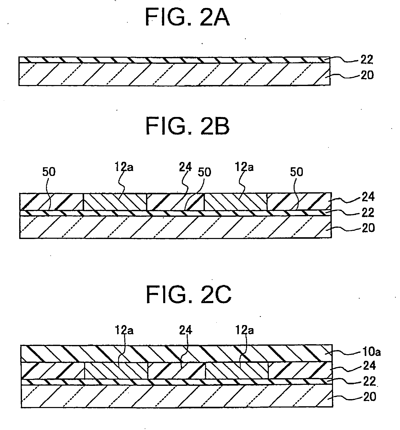
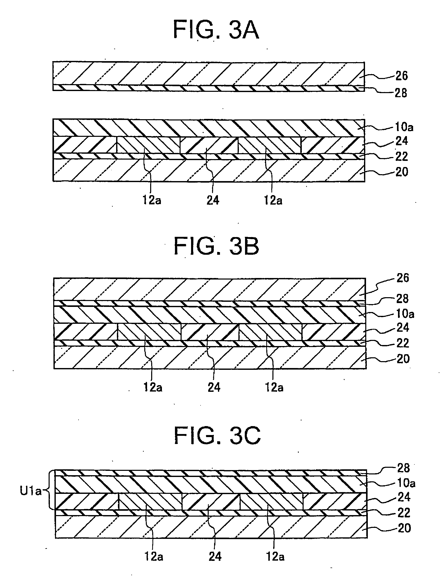
[0044]The release layer paste of the present invention contains polyvinyl acetal as the main ingredient in the binder forming the paste. The polyvinyl acetal contained in the paste in the present invention is hard to be dissolved or swelled by (is hardly soluble with) the solvent in the electrode layer paste or blank pattern layer paste for forming the electrode layer or blank pattern layer, that is, the limonene, dihydroterpinyl methyl ether, α-terpinyl acetate, terpinyl methyl ether, isobornyl acetate, caryophyllene, 1-dihydrocarvyl acetate, menthone, menthyl acetate, perillyl acetate, carvyl acetate, d-dihydrocarvyl acetate, or butyl carbitol acetate. For this reason, the release layer formed using the release layer paste of the present invention has the effect of being free from sheet attack from the electrode layer paste or blank pattern layer paste. As a result, the printability of the electrode layer paste or blank pattern layer paste for forming the electrode layer or blank pattern layer with respect to the release layer formed using the release layer paste of the present invention is stable. Specifically, it is possible to prevent the occurrence of bleedout, shedding, and pinholes of the electrode layer or blank pattern layer formed on the surface of the release layer. Bleedout, shedding, and pinholes of the electrode layer or blank pattern layer easily occurs due to exposure of the surface of the supporting sheet due to the dissolution of the release layer. The release layer formed using the release layer paste of the present invention is free from sheet attack from the electrode layer paste or blank pattern layer paste, so there is no occurrence of bleedout, shedding, and pinholes of the electrode layer or blank pattern layer formed on the surface of the release layer.
[0045]In particular, in the present invention, since the above solvents is used as the solvent contained in the electrode layer paste or blank pattern layer paste used in combination, even if the release layer is made a thin 0.1 μm or less, the occurrence of sheet attack and the occurrence of bleedout, shedding, and pinholes of the electrode layer or blank pattern layer can be effectively prevented. For this reason, the release layer can be made thinner. Due to this, the dielectric layer can be made thinner for the following reasons.
[0048]Therefore, to make the dielectric layer thinner, while to realize the desired dielectric characteristics, for making the multilayer electronic device smaller in size and higher in performance, it is important to reduce the thickness of the release layer as much as possible.
[0050]In the present invention, preferably the peeling strength of the first supporting sheet is controlled to 8 to 20 mN / cm (however, excluding 8 mN / cm), whereby even if used combined with an electrode layer paste using the above solvents, the release layer formed using the release layer paste of the present invention will not drop off from the first supporting sheet.

Problems solved by technology

In the process of production of such electronic devices, the thicknesses of the green sheets able to form the dielectric layers after firing have become extremely thin (usually 1.5 μm or less), so at the time of formation of the electrode layers by the printing method, the solvent of the electrode layer paste causes the green sheets to dissolve, that is, the so-called “sheet attack” phenomenon becomes a problem.
This sheet attack phenomenon leads directly to defects of the green sheets and short-circuit defects, so is a problem which absolutely must be solved for making the layers thinner.
However, Japanese Patent Publication (A) No. 63-51616, Japanese Patent Publication (A) No. 3-250612, and Japanese Patent Publication (A) No. 7-312326 had the problem of a difficulty of peeling off the predetermined pattern of the electrode layer from the supporting film.
However, if using an electrode layer paste using terpineol or dehydroterpineol as a solvent together with a release layer using a butyral resin as a binder, the solvent of the electrode layer paste causes sheet attack at the release layer.
Sheet attack of the release layer becomes a cause of bleedout, shedding, and pinholes at the electrode layer or blank pattern layer formed on the surface of the release layer.
This in turn can increase the short-circuit defects of the final multilayer type electronic device.

Method used


Image

  • Release layer paste and method of production of a multilayer type electronic device
  • Release layer paste and method of production of a multilayer type electronic device
  • Release layer paste and method of production of a multilayer type electronic device

Examples


example 1

[0158]Preparation of Release Layer Paste

[0159]Preparation of Additive Slurry

[0160]First, as the additive (subcomponent) materials, (Ba,Ca) SiO3 in an amount of 1.48 parts by weight, Y2O3 in 1.01 parts by weight, MgCO3 in 0.72 part by weight, MnO in 0.13 part by weight, and V2O5 in 0.045 part by weight were prepared. Next, the prepared additive (subcomponent) materials were mixed to obtain the additive (subcomponent) material mixture.

[0161]Next, the additive material mixture in an amount of 8.75 parts by weight was mixed and pulverized with ethyl alcohol in 6.21 parts by weight, n-propanol in 6.21 parts by weight, xylene in 2.19 parts by weight, and a polyethylene glycol-based dispersion agent in 0.09 part by weight using a ball mill to obtain an additive slurry. The mixing and pulverization were performed using a 250 cc polyethylene resin vessel charged with 450 g of 2 mmφ ZrO2 media at a peripheral speed of 45 m / min for 20 hours. The pulverized additive material had a particle size...

example 2

[0198]Except for making the dry thickness of the release layer 0.07 μm, the same procedure was followed as in Example 1 to form and evaluate the release layer. The results are shown in Table 2.

example 3

[0199]Except for making the dry thickness of the release layer 0.05 μm, the same procedure was followed as in Example 1 to form and evaluate the release layer. The results are shown in Table 3.


PUM

PropertyMeasurementUnit
Lengthaaaaaaaaaa
Percent by massaaaaaaaaaa

Abstract

A release layer paste used for producing a multilayer type electronic device and forming a release layer of a thickness of 0.05 to 0.1 μm, used in combination with an electrode layer paste including one or more solvents selected from limonene, dihydroterpinyl methyl ether, α-terpinyl acetate, terpinyl methyl ether, isobornyl acetate, caryophyllene, 1-dihydrocarvyl acetate, menthone, menthyl acetate, perillyl acetate, carvyl acetate, d-dihydrocarvyl acetate, and butyl carbitol acetate and a binder comprised of ethyl cellulose, including a ceramic powder, organic vehicle, plasticizer, and dispersion agent, the organic vehicle containing a binder having polyvinyl acetal as its main ingredient, a ratio (P / B) of the ceramic powder with respect to the binder and plasticizer being controlled to 1.33 to 5.56 (however, excluding 5.56).

Description

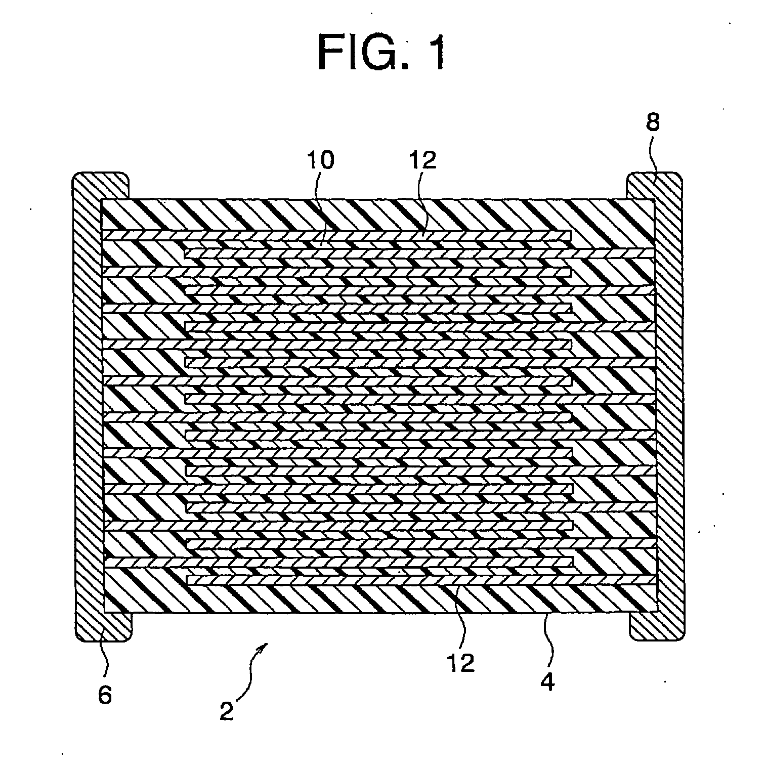
BACKGROUND OF THE INVENTION[0001]1. Field of the Invention[0002]The present invention relates to release layer paste used for production of a multilayer ceramic capacitor or other multilayer type electronic device and a method of production of a multilayer type electronic device using the release layer paste.[0003]2. Description of the Related Art[0004]In recent years, due to the increasingly smaller sizes of electronic apparatuses, multilayer ceramic capacitors and other multilayer type electronic devices have become increasingly compact in size and sophisticated in performance. The thicknesses of the interlayer dielectric layers of multilayer type electronic devices (dielectric layers sandwiched between pairs of internal electrodes) have become 1 μm or less—enabling over 800 stacked layers. In the process of production of such electronic devices, the thicknesses of the green sheets able to form the dielectric layers after firing have become extremely thin (usually 1.5 μm or less),...

Claims


Application Information

Patent Timeline
IPC IPC(8): B05D5/00B05D3/02C09D5/20
CPCC09D5/20Y10T428/252H01G4/30H01G4/1209H01G4/008
Inventor ABE, KYOTAROSATO, SHIGEKI
Owner TDK CORPARATION
Why Eureka
Eureka Blog
Learn More