Chip package and method for fabricating the same

a technology of chip and aluminum pad, applied in the field of chip package, can solve the problem of easy damage to the original aluminum pad

Active Publication Date: 2007-09-06
SUMITOMO ELECTRIC IND LTD +1
View PDF75 Cites 183 Cited by
  • Summary
  • Abstract
  • Description
  • Claims
  • Application Information

AI Technical Summary

Problems solved by technology

If solder bumps and wirebonds are to be formed on a same chip, some damage to original aluminum pad could easily occur when an under bump metallurgy (UBM) layer acting with an adhesion function and a barrier function is formed on the original pads for solder bumps.

Method used


Image

  • Chip package and method for fabricating the same
  • Chip package and method for fabricating the same
  • Chip package and method for fabricating the same

Examples


embodiment 1

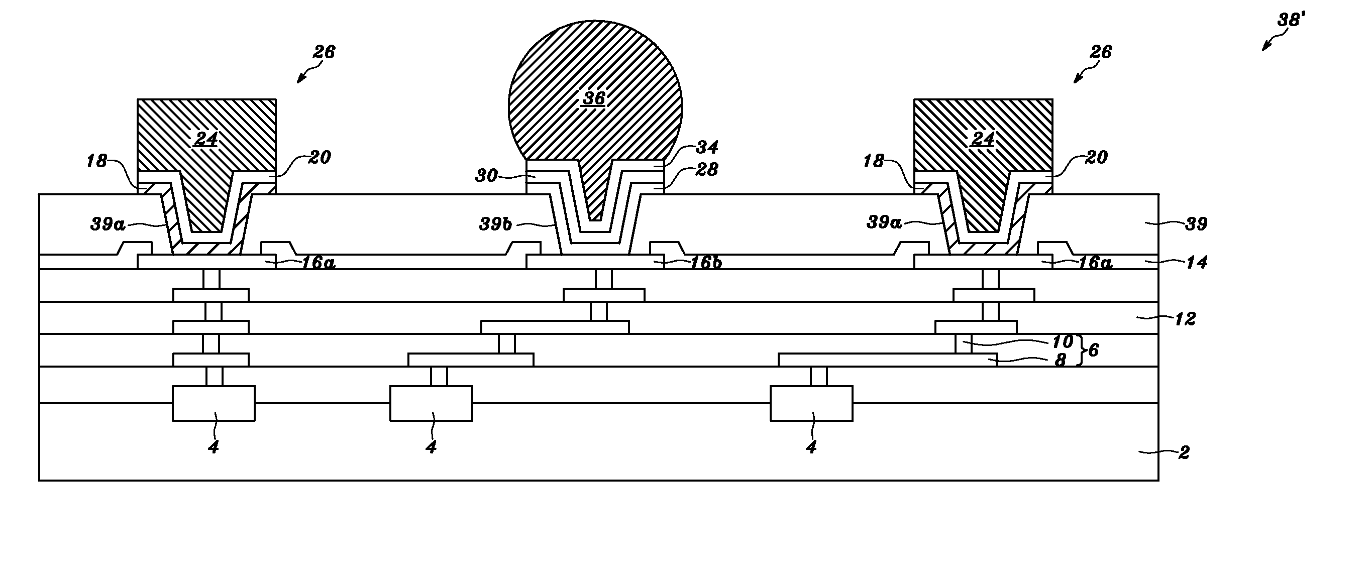
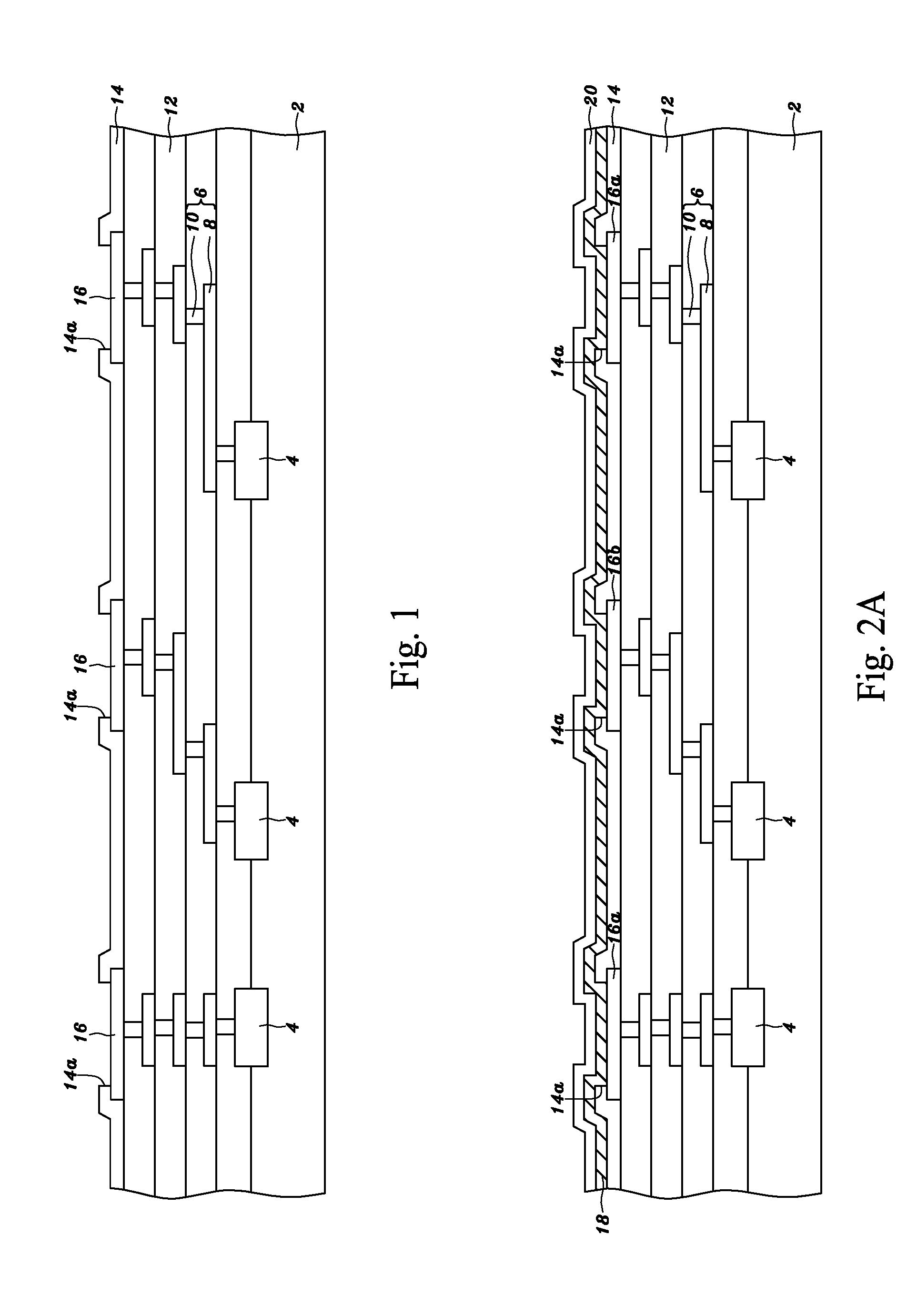
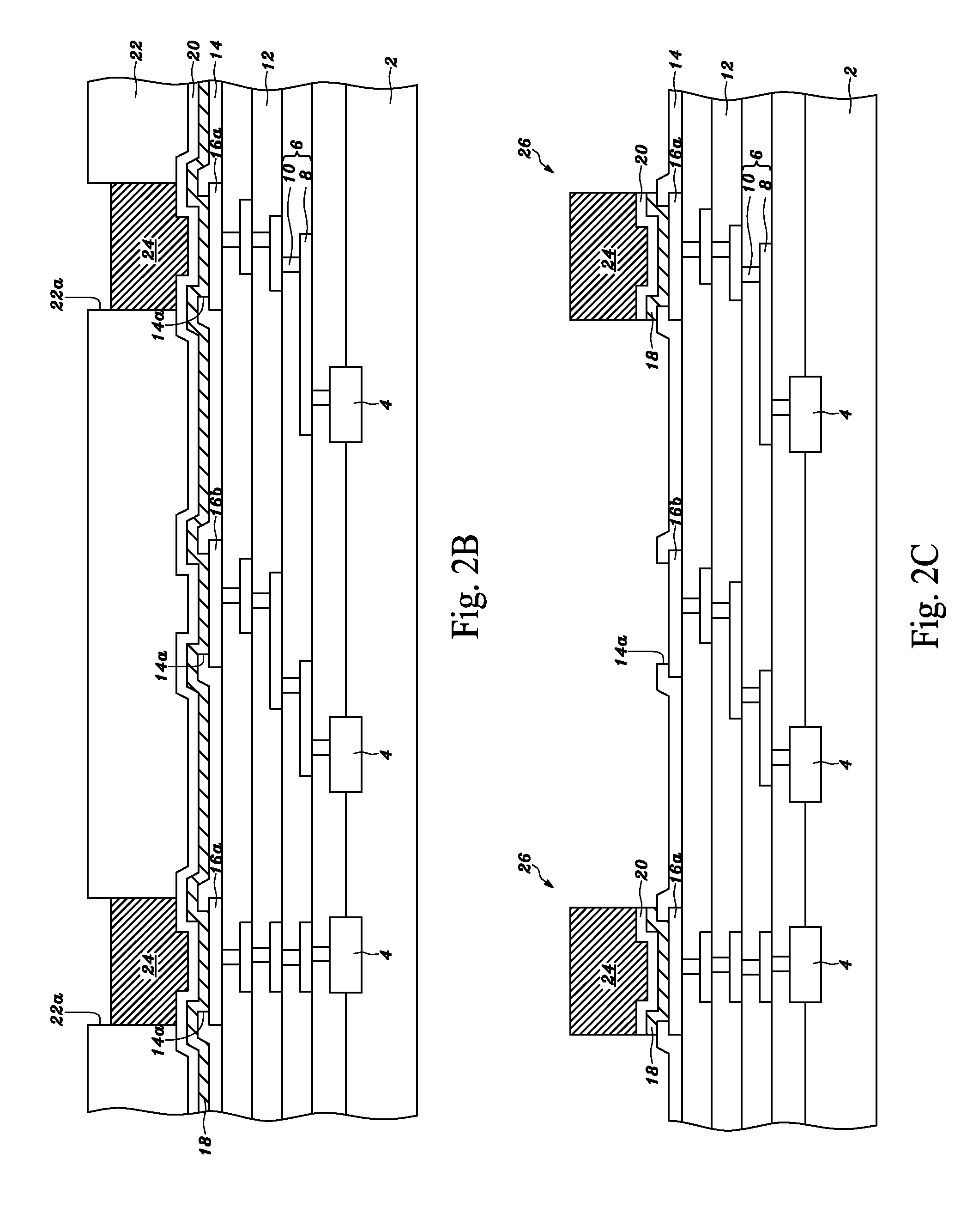
[0047]FIG. 2A to FIG. 2H are schematic cross-sectional views showing a method for forming a tin-containing metal layer or bump and a metal pad or bump over a semiconductor wafer.

[0048] Referring to FIG. 2A, the bonding pads 16 comprise multiple first bonding pads 16a (only two is shown) and multiple second bonding pads 16b (only one is shown). An adhesion / barrier layer 18 having a thickness of 0.01 and 3 μm is formed on the passivation layer 14, on the first bonding pad 16a exposed by the opening 14a, and on the second bonding pad 16b exposed by the opening 14a. The thickness of the adhesion / barrier layer 18 is preferred to be between 0.01 and 1 μm. The material of the adhesion / barrier layer 18 may include titanium, tungsten, cobalt, nickel, titanium nitride, a titanium-tungsten alloy, a nickel-vanadium alloy, aluminum, chromium, copper, gold, protactinium, platinum, palladium, ruthenium, rhodium, silver, or a composite of the above mentioned materials. The adhesion / barrier layer 1...

embodiment 2

[0077] Embodiment 1 can apply to a RDL (Re-Distribution Layer) or an interconnecting trace. Below is to be described an embodiment, wherein a RDL and an interconnecting trace are simultaneously formed over a semiconductor substrate. However, the present invention also includes the case: only a RDL or interconnecting trace is formed over a semiconductor substrate, and a metal pad or bump and a tin-containing metal layer or bump are then formed on the RDL or interconnecting trace.

[0078] Referring to FIG. 3C, a metal trace 40 functioning as a redistribution layer (RDL) is formed over a passivation layer 44 and connected to a bonding pad 46 exposed by an opening 44a in the passivation layer 44. A metal trace 42 functioning as an interconnecting trace is formed over the passivation layer 44 and connects multiple of to the bonding pads 46 exposed by the openings 44a in the passivation layer 44. Refer to the foregoing description of the passivation layer 14 and the bonding pad 16 for the ...

embodiment 3

[0107]FIG. 5A to FIG. 5H are schematic cross-sectional views showing a method for forming a tin-containing metal layer or bump and a metal pad or bump over a semiconductor wafer.

[0108] Referring to FIG. 5A, after the adhesion / barrier layer 18 shown in FIG. 2A is formed, a seed layer 20′ is formed on the adhesion / barrier layer 18, wherein the seed layer 20′ has a thickness of between 0.005 and 10 μm with a preferred thickness of between 0.01 and 2 μm. The seed layer 20′ may be formed by a sputtering method, a vapor deposition method, an electroplating method, an electroless plating method or a PVD method. The seed layer 20′ is beneficial to electroplating a metal layer thereon. Thus, the material of the seed layer 20′ varies with the material of the succeeding metal layer formed on the seed layer 20′. When a copper metal layer is to be electroplated on the seed layer 20′, copper is a preferable material to the seed layer 20′. When a gold metal layer is to be electroplated on the see...


PUM

PropertyMeasurementUnit
thicknessaaaaaaaaaa
thicknessaaaaaaaaaa
thicknessaaaaaaaaaa

Abstract

A chip package includes a semiconductor substrate, a first metal pad over the semiconductor substrate, and a second metal pad over the semiconductor substrate. In a case, the first metal pad is tape automated bonded thereto, and the second metal pad is solder bonded thereto. In another case, the first metal pad is tape automated bonded thereto, and the second metal pad is wirebonded thereto. In another case, the first metal pad is solder bonded thereto, and the second metal pad is wirebonded thereto. In another case, the first metal pad is bonded to an external circuitry using an anisotropic conductive film, and the second metal pad is solder bonded thereto. In another case, the first metal pad is bonded to an external circuitry using an anisotropic conductive film, and the second metal pad is wirebonded thereto.

Description

[0001] This application claims priority to U.S. provisional application No. 60 / 767,080, filed on Mar. 2, 2006, which are herein incorporated by reference in their entirety.BACKGROUND OF THE INVENTION [0002] 1. Field of the Invention [0003] The present invention relates to a chip package and a method for fabricating the same. More particularly, the present invention relates to a chip package having two different kinds of metal pads over a same semiconductor substrate and a method for forming the same. [0004] 2. Brief Description of the Related Art [0005] At present, the market for multimedia applications is expanding rapidly. The integrated circuit (IC) packaging techniques, therefore, also need to be able to accommodate the developing trends of electronic devices, such as, digitalization, networking, localization, and user friendliness. In order to meet the above requirements, electronic devices must be multifunctional, highly integrated, miniaturized and light weighted, inexpensive...

Claims


Application Information

Patent Timeline
Patent Type & Authority Applications(United States)
IPC IPC(8): H01L23/48
CPCH01L23/3157H01L23/4985H01L23/66H01L24/03H01L24/05H01L24/06H01L24/11H01L24/12H01L24/16H01L24/45H01L24/48H01L24/73H01L25/0657H01L2224/0401H01L2224/04042H01L2224/04073H01L2224/05024H01L2224/05124H01L2224/05147H01L2224/05155H01L2224/05558H01L2224/05568H01L2224/05572H01L2224/05644H01L2224/05655H01L2224/1147H01L2224/11902H01L2224/11912H01L2224/13022H01L2224/13139H01L2224/13144H01L2224/13147H01L2224/13155H01L2224/13164H01L2224/13169H01L2224/13173H01L2224/13176H01L2224/13183H01L2224/45144H01L2224/45147H01L2224/4807H01L2224/48091H01L2224/48145H01L2224/48463H01L2225/06506H01L2225/06513H01L2225/06517H01L2225/06579H01L2924/01006H01L2924/01007H01L2924/01011H01L2924/01013H01L2924/01014H01L2924/01015H01L2924/01018H01L2924/01022H01L2924/01027H01L2924/01028H01L2924/01029H01L2924/01046H01L2924/01047H01L2924/01049H01L2924/0105H01L2924/01073H01L2924/01074H01L2924/01075H01L2924/01078H01L2924/01079H01L2924/01082H01L2924/014H01L2924/04941H01L2924/04953H01L2924/05042H01L2924/09701H01L2924/10329H01L2924/12044H01L2924/14H01L2924/19041H01L2924/19042H01L2924/19043H01L2924/00013H01L2924/01019H01L2924/01023H01L2924/01024H01L2924/01033H01L2924/01044H01L2924/01045H01L2924/01072H01L2224/05027H01L2224/05559H01L2224/48453H01L2224/48644H01L2224/48655H01L2224/48844H01L2224/48855H01L2224/73204H01L2924/1305H01L2924/0002H01L2924/00014H01L2224/13099H01L2924/00H01L2224/05552H01L2924/15787H01L2924/181H01L2224/1403H01L2224/14051H01L2224/14505H01L2224/06102H01L2924/00012
Inventor CHOU, CHIEN-KANGCHOU, CHIU-MINGLIN, LI-RENLO, HSIN-JUNG
Owner SUMITOMO ELECTRIC IND LTD
Why Eureka
Try Eureka