Cooling block forming electrode

a technology of cooling block and electrode, which is applied in the field of cooling block forming electrode, can solve the problems of corroding the inner peripheral surface of the channel b>14/b>, cracking of the alumite coating film, and blockage of the cooling liquid in the channel

Inactive Publication Date: 2007-09-13
TOKYO ELECTRON LTD
View PDF4 Cites 18 Cited by
  • Summary
  • Abstract
  • Description
  • Claims
  • Application Information

AI Technical Summary

Benefits of technology

[0020] According to the present invention, it is easy to form the channel for a cooling liquid out of stainless (SUS). The stainless channel i

Problems solved by technology

However, when aluminum is used, since an aluminum solid surface is exposed to the cooling liquid channel 14 which is in contact with a cooling liquid, there is a possibility that an inner peripheral surface of the channel 14 is corroded by the cooling liquid circulating therethrough.
The corrosion of the inner peripheral surface of the channel 14 may then result in a blockage of the cooling liquid in the channel 14.
However, in joining the metal plates whose surfaces have been subjected to an alumite coating process before brazing, there is concern that an alumite coating film is cracked if the alumite coating film cannot resist a brazing temperature.
The cracked alumite coating film cannot fully achieve an anti-corrosion function.
Howev

Method used


Image

  • Cooling block forming electrode
  • Cooling block forming electrode
  • Cooling block forming electrode

Examples


first embodiment

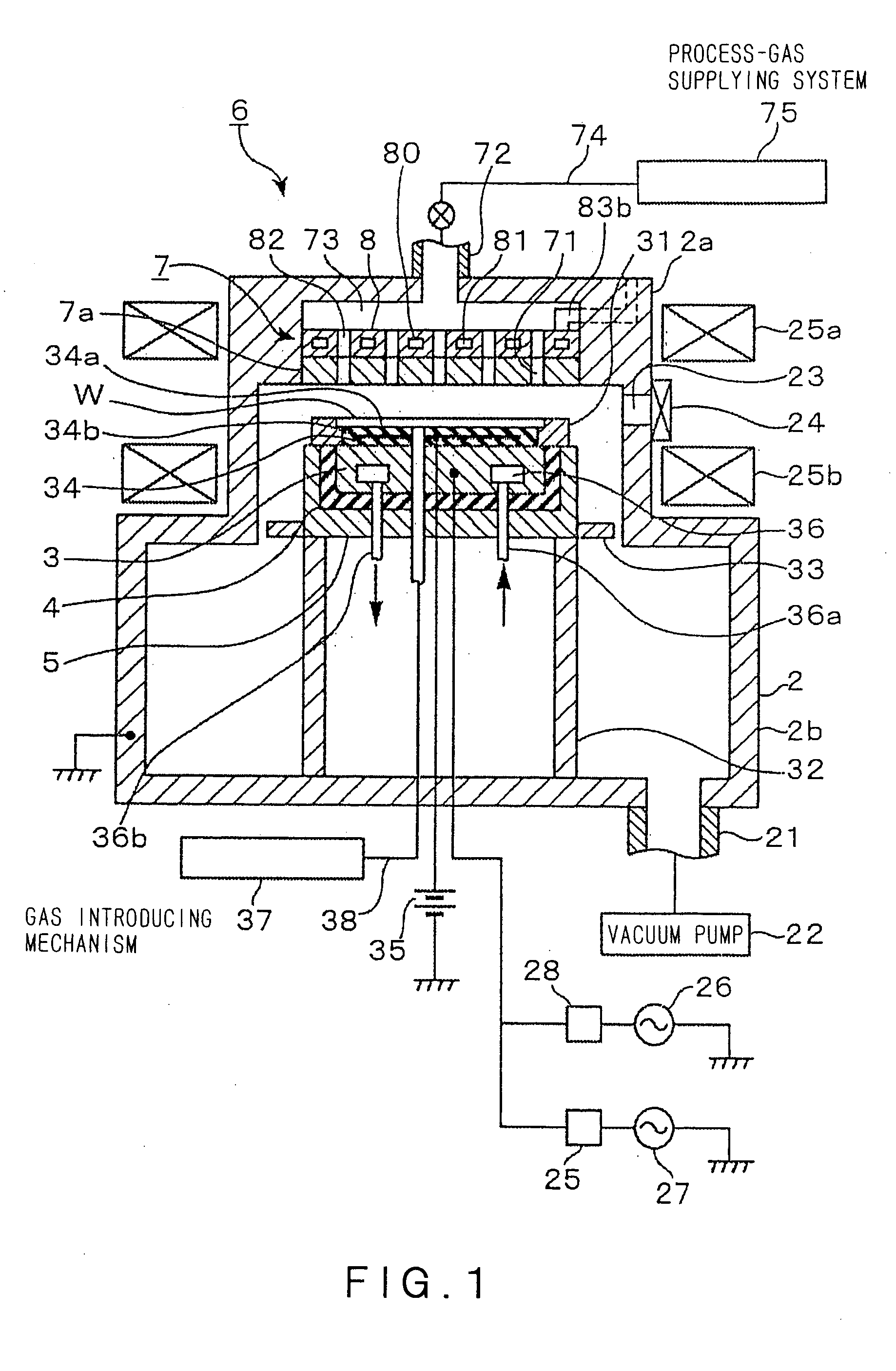
[0037]FIG. 1 is a schematic sectional view of an RIE (Reaction Ion Etching) plasma etching apparatus including a cooling block in a first embodiment of the present invention. As shown in FIG. 1, the plasma etching apparatus in this embodiment includes a process vessel 2 (vacuum chamber) made of, e.g., aluminum. The process vessel 2, which has an upper cylindrical part 2a of a smaller diameter and a lower cylindrical part 2b of a larger diameter, can be hermetically sealed.

[0038] In the process vessel 2, there is disposed a support table 3, which supports horizontally a semiconductor wafer W (hereafter referred to as “wafer”) as a substrate to be processed and also serves as a lower electrode. The support table 3 is made of, e.g., aluminum, and is supported by a conductive support base 5 via an insulating plate 4. A focus ring 31 made of, e.g., silicon (Si) is disposed on an upper periphery of the supporting table 3. A lower part of the support base 5 is covered with a cover 32. A b...

second embodiment

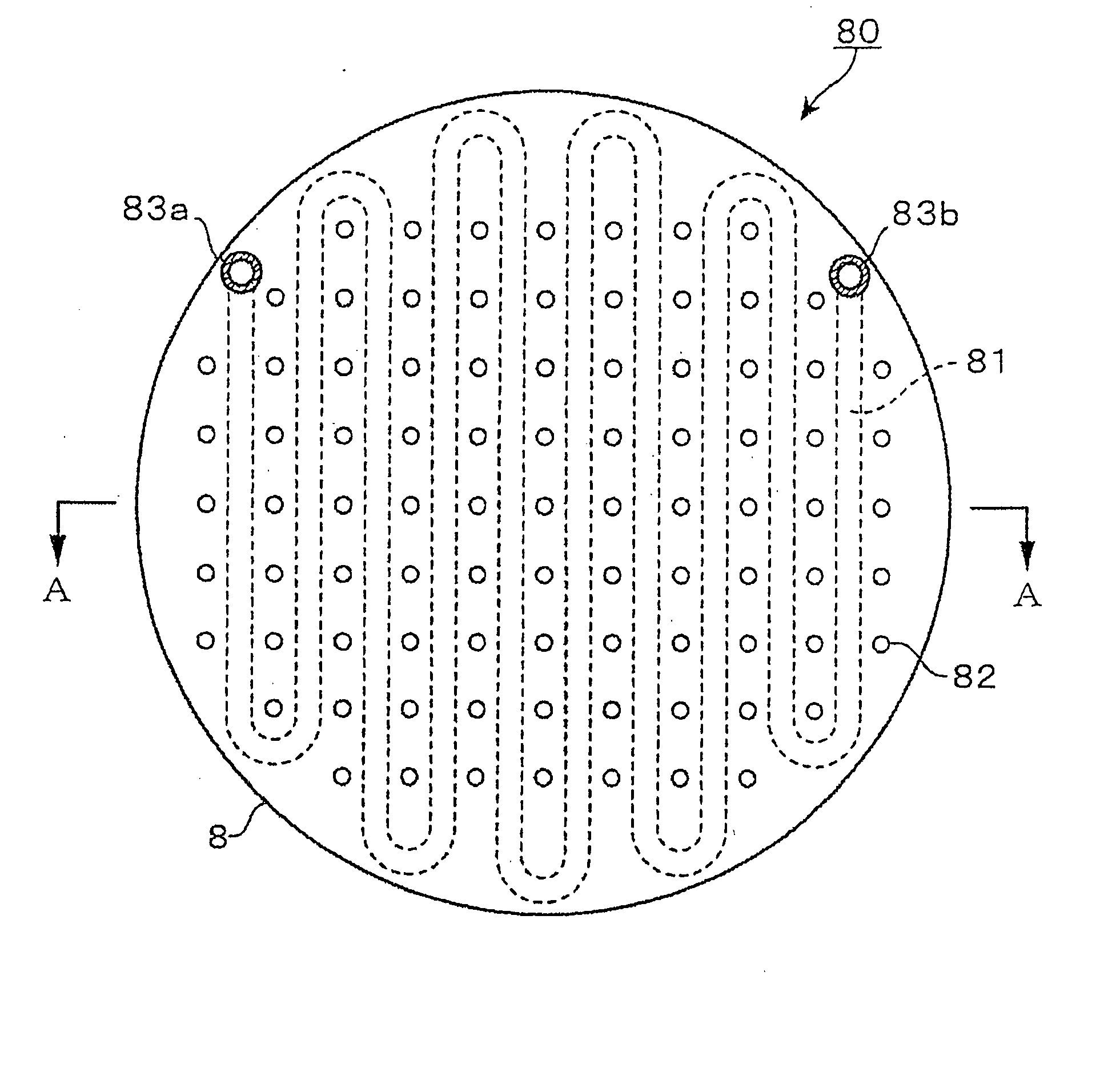
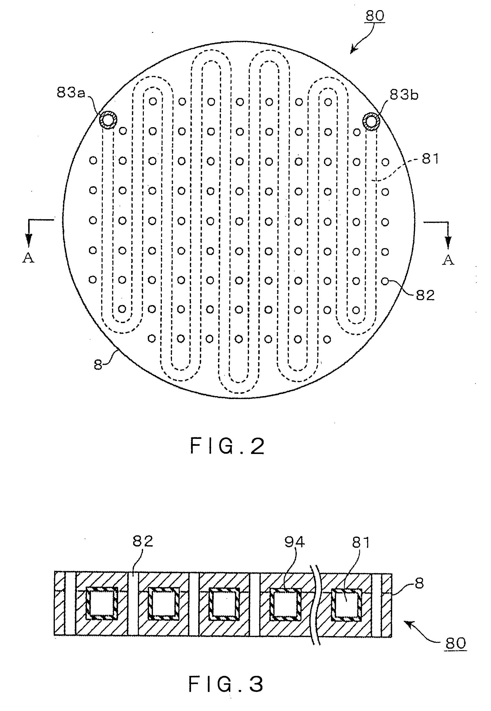
[0065] In a cooling block in a second embodiment of the present invention, an inner surface of a channel 81 formed in a base material 8 is entirely covered with stainless steel (SUS).

[0066] A manufacturing method of such cooling block 90 is concretely described with reference to FIGS. 6A to 7D.

[0067] At first, as shown in FIGS. 6A and 6B, a lower plate 94a made of SUS is processed to have, e.g., parallel grooves as recesses 80a for forming a channel. Holes 95 are drilled in ridges 80b between the grooves in the lower plate 94a. A diameter of the hole 95 is larger than that of a gas jetting hole formed in a base material, which is described below. A flat upper plate 94b made of SUS is also provided with the holes 95, each having a diameter larger than the hole formed in the base material, which is described below. The holes 95 drilled in the lower plate 94a and the holes 95 drilled in the upper plate 94b are arranged so as to correspond to each other, when the lower plate 94a and t...

example 1

[0079] A test block corresponding to the cooling block 80 was manufactured in accordance with the same procedures as those of the first embodiment (see, FIGS. 4A to 5C).

[0080] An amount of zinc applied to the surface of the first base material 8a was 30 g per 1 m2. A brazing material containing 80% or more by weight of Ni was applied to the surface of the second base material 8b. The cooling block manufactured as above is called Example 1.


PUM

PropertyMeasurementUnit
Massaaaaaaaaaa
Areaaaaaaaaaaa
Thicknessaaaaaaaaaa

Abstract

The present invention is a cooling block that forms an electrode for generating a plasma for use in a plasma process, and includes a channel for a cooling liquid, the cooling block comprising: a first base material and a second base material respectively made of aluminum, at least one of the first and second base materials having a recess for forming a channel for a cooling liquid; and a diffusion bonding layer, in which zinc is diffused in aluminum, and an anti-corrosion layer of a zinc oxide film, the layers being formed by interposing zinc between the first and second base materials, and by bonding the first and second base materials with zinc interposed therebetween in a heating atmosphere containing oxygen.

Description

FIELD OF THE INVENTION [0001] The present invention relates to a cooling block forming an electrode for generating a plasma for use in a plasma process, and to a plasma processing apparatus using the cooling block. BACKGROUND ART [0002] In a process for manufacturing semiconductor devices or the like, a plasma process using a plasma is frequently performed. As shown in FIG. 9, a plasma processing apparatus for the plasma process includes, for example, a process vessel 10 of a vacuum chamber, and a stage 11 disposed in the process vessel 10 for supporting thereon a semiconductor wafer (hereafter referred to as “wafer”) as a substrate. The stage 11 also serves as a lower electrode. A showerhead 12 having a number of gas supply holes 12a is arranged above the stage 11. An upper electrode 13 is disposed on a lower surface of the showerhead 12. The upper electrode 13 is formed of an electrode plate 13a and a cooling block 13b. [0003] A radio-frequency for generating plasma is applied bet...

Claims


Application Information

Patent Timeline
IPC IPC(8): B23K9/00
CPCH01J37/32009H05H1/46H01J37/32724
Inventor ISHIDA, TOSHIFUMIHAYASHI, DAISUKE
Owner TOKYO ELECTRON LTD
Why Eureka
Try Eureka