Photomask blank and photomask

a technology of photomask and photomask, which is applied in the field of photomask blank and photomask, can solve the problems of preventing effective pattern transfer, degrading resist pattern profile, and increasing demand for circuit pattern miniaturization, and achieves phase control, high accuracy, and reduced pattern density dependency

Active Publication Date: 2007-09-13
SHIN ETSU CHEM IND CO LTD +1
View PDF23 Cites 105 Cited by
  • Summary
  • Abstract
  • Description
  • Claims
  • Application Information

AI Technical Summary

Benefits of technology

[0017]An object of the invention is to provide a photomask blank which endows a photomask with both a high resolution and a high accuracy etching capability for forming a finer photomask pattern, especially as needed in the photolithography involving exposure to light of a wavelength equal to or less than 250 nm such as ArF excimer laser light, i.e., a photomask blank having a sufficient process accuracy of etch processing to form a pattern with minimized pattern density dependency, or even a photomask blank having a minimized possibility of causing damages to a phase shift film and a transparent substrate below the light-shielding film during removal of the light-shielding film and a processing accuracy substantially equivalent to that attainable with the prior art light-shielding films of chromium-based material; and a photomask obtained by patterning the photomask blank.
[0018]Regarding the accuracy of etch processing to a pattern with a size equal to or less than 0.4 μm, the inventors have found the following. Even a film of chromium-based material can be reduced in pattern density dependency if it is made fully thin, but a chromium-based material film within such thickness range is short in light shielding. As compared with the dry etching of chromium-based materials under chlorine and oxygen-containing conditions, a film which can be processed by fluorine dry etching exhibits reduced pattern density dependency during fluorine dry etching, so that the film can be precision processed even at a sufficient thickness to serve as a light-shielding film. A film containing a transition metal and silicon is appropriate to this end.
[0019]Even a film of chromium-based material has reduced pattern density dependency if it is fully thin. Then the chromium-based material film can be utilized in precision processing of patterns if the film has a minimum thickness so that it has no impact on optical properties (e.g., transmittance) of a pattern formed on a photomask.
[0020]On the basis of these findings, the inventors have found the following. A light-shielding film consists of a single layer composed of a material containing a transition metal and silicon or multiple layers including at least one layer composed of a material containing a transition metal and silicon; an etch stop film is disposed on a transparent substrate, optionally with another film intervening therebetween, and particularly when a phase shift film is to be used, the phase shift film intervening therebetween, the etch stop film of single layer or multilayer construction being resistant to fluorine dry etching and removable by chlorine dry etching, preferably the etch stop film being composed of chromium alone or a chromium compound containing a transition metal and at least one element of oxygen, nitrogen and carbon; the light-shielding film is disposed contiguous to the etch stop film; and an antireflective film consisting of a single layer or multiple layers is disposed on the light-shielding film. The lamination of films as above results in a photomask blank having the advantages that the light-shielding film can be processed at a high accuracy independent of the pattern density, the light-shielding film can be removed without causing damages to the transparent substrate and phase shift film, and even when the phase shift film and transparent substrate are processed by etching after formation of a pattern of the light-shielding film, a pattern can be transferred to the phase shift film and transparent substrate at a high accuracy.
[0030]As compared with photomask blanks having conventional light-shielding films of chromium-based materials, the photomask blank of the invention has the advantage that when the light-shielding film is dry etched to form a pattern, the variation of pattern feature size arising from the pattern density dependency is reduced. This enables to produce a mask at a high accuracy. When the photomask blank of the invention is applied to a halftone phase shift mask, chromeless mask or Levenson mask, the light-shielding film can be selectively removed by dry etching without causing damages to any film underlying the light-shielding film and transparent substrate, enabling phase control at a high accuracy. Then photomasks for super-resolution exposure can be manufactured at a high accuracy.

Problems solved by technology

In the recent semiconductor processing technology, a challenge to higher integration of large-scale integrated circuits places an increasing demand for miniaturization of circuit patterns.
As a result, the resist pattern profile is degraded, preventing effective pattern transfer, and in some cases, there occurs resist pattern collapse or stripping.
If etching is carried out through a thin resist film, accurate transfer of the resist pattern is difficult.
It is a task of some difficulty for the resist to have both a high resolution and etch resistance that allows for high accuracy etching.
Also, JP-A 4-246649 discloses a metal silicide film, which has not been applied to the actual fabrication because of some practical problems.

Method used


Image

  • Photomask blank and photomask
  • Photomask blank and photomask
  • Photomask blank and photomask

Examples


example

[0178]Experiments and Examples are given below for further illustrating the invention although the invention is not limited thereto.

[0179]In Examples, fluorine dry etching was performed by feeding only C2F6 gas into a chamber at a flow rate of 20 sccm, and setting a pressure of 2 Pa in the chamber. Chlorine dry etching is performed by feeding chlorine gas at a flow rate of 20 sccm, oxygen gas at 20 sccm and helium gas at 80 sccm into a chamber, and setting a pressure of 2 Pa in the chamber.

experiment 1

[0180]By selecting one of targets containing molybdenum and silicon in an atomic ratio of 0:100, 1:15, 1:9, 1:4, 1:2, and 1:1 and sputtering the target in an argon atmosphere, a molybdenum silicide film of 39 nm thick was deposited (the film having a molybdenum / silicon ratio corresponding to the selected target). The molybdenum silicide films were immersed in aqueous ammonia / hydrogen peroxide (aqueous ammonia:hydrogen peroxide:water=1:1:30 in volume ratio) for one hour, after which a change of film thickness was determined. The film thickness losses were 0.2, 0.2, 0.7, 1.5, 17.7, and 39 nm, respectively. The films were also measured for electric conductivity using a four-probe sheet resistance meter MCP-T600 (Mitsubishi Chemical Co., Ltd.), finding conductivity values of 1082, 680, 486, 296, 96, and 38 ohm / square (Ω / □), respectively.

[0181]With regard to these materials for light-shielding film and antireflective film (ARF), it was found that when the ratio of transition metal to sil...

example 1

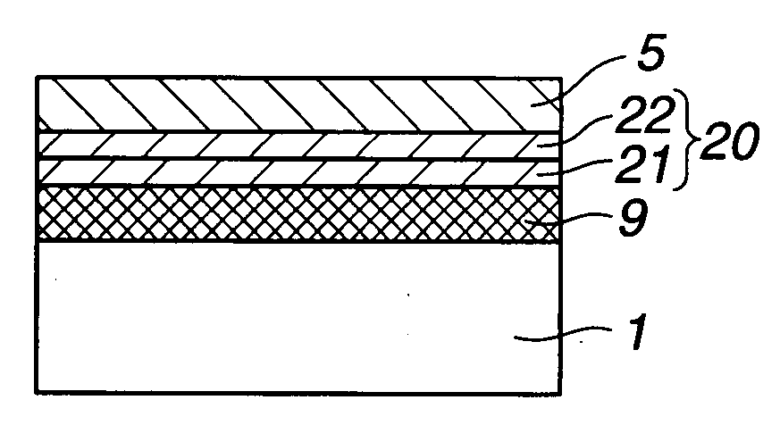
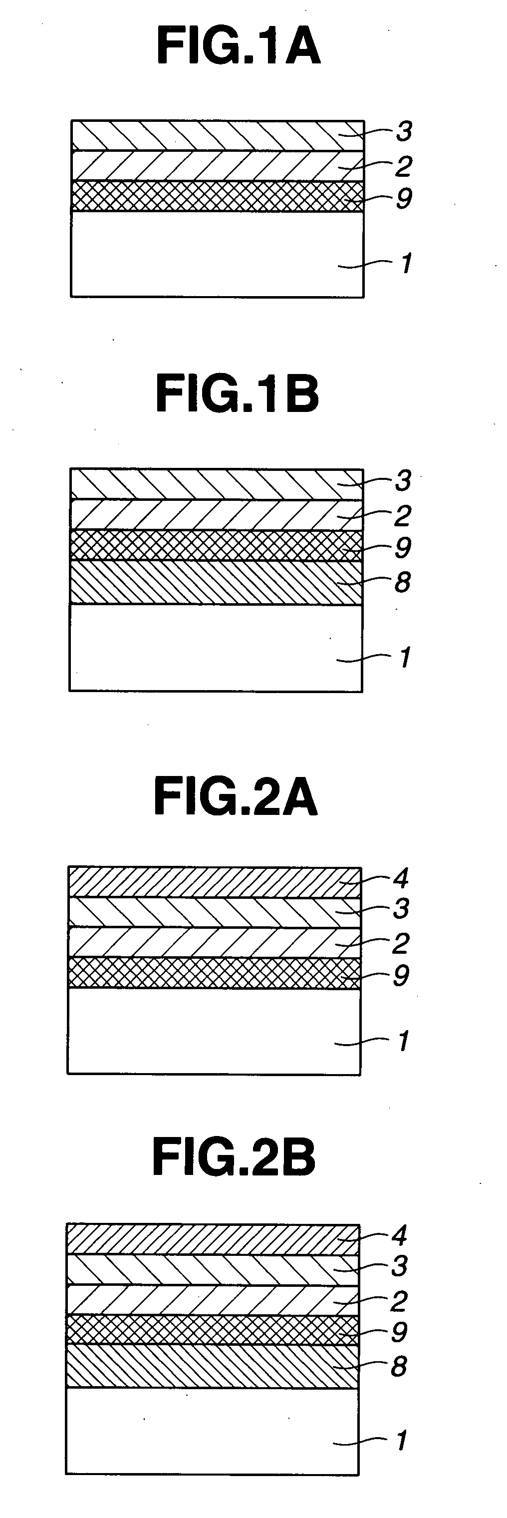
[0182]A photomask blank having the layer arrangement shown in FIG. 1A was prepared by depositing the films by sputtering. The respective films are as follows.[0183]Transparent substrate: quartz substrate[0184]Etch stop film: CrN (Cr:N=9:1 in atomic ratio, thickness 10 nm)[0185]Light-shielding film: MoSi (Mo:Si=1:4 in atomic ratio, thickness 41 nm)[0186]ARF: MoSiN (thickness-wise compositional grading from Mo:Si:N=1:3:1.5 in atomic ratio on light-shielding film side to Mo:Si:N=1:5:5 in atomic ratio on side remote from transparent substrate (surface side), thickness 18 nm)

[0187]This photomask blank was processed in accordance with photomask manufacturing process A, whereby a Levenson mask was produced. For the first and second resist films, a chemically amplified negative resist mainly comprising a hydroxystyrene resin, a crosslinker, and a photoacid generator was used to form a resist film of 250 nm thick. The resist films were patterned by EB lithography. Before formation of the fir...


PUM

PropertyMeasurementUnit
thicknessaaaaaaaaaa
thicknessaaaaaaaaaa
thicknessaaaaaaaaaa

Abstract

A photomask blank is provided comprising an etch stop film which is disposed on a transparent substrate and is resistant to fluorine dry etching and removable by chlorine dry etching, a light-shielding film disposed on the etch stop film and including at least one layer composed of a transition metal / silicon material, and an antireflective film disposed on the light-shielding film. When the light-shielding film is dry etched to form a pattern, pattern size variation arising from pattern density dependency is reduced, so that a photomask is produced at a high accuracy.

Description

CROSS-REFERENCE TO RELATED APPLICATION[0001]This non-provisional application claims priority under 35 U.S.C. §119(a) on Patent Application No. 2006-065800 filed in Japan on Mar. 10, 2006, the entire contents of which are hereby incorporated by reference.TECHNICAL FIELD[0002]This invention relates to photomask blanks from which are produced photomasks for use in the microfabrication of semiconductor integrated circuits, charge coupled devices (CCD), liquid crystal display (LCD) color filters, magnetic heads or the like, and photomasks produced therefrom.BACKGROUND ART[0003]In the recent semiconductor processing technology, a challenge to higher integration of large-scale integrated circuits places an increasing demand for miniaturization of circuit patterns. There are increasing demands for further reduction in size of circuit-constructing wiring patterns and for miniaturization of contact hole patterns for cell-constructing inter-layer connections. As a consequence, in the manufactu...

Claims


Application Information

Patent Timeline
Patent Type & Authority Applications(United States)
IPC IPC(8): B32B9/00B32B17/10B32B17/06G03F1/00G03F1/32G03F1/68
CPCG03F1/32G03F1/46G03F1/58G03F1/80Y10T428/31616G03F1/38G03F1/28G03F1/30G03F1/62
Inventor YOSHIKAWA, HIROKIINAZUKI, YUKIOOKAZAKI, SATOSHIHARAGUCHI, TAKASHISAGA, TADASHIKOJIMA, YOSUKECHIBA, KAZUAKIFUKUSHIMA, YUICHI
Owner SHIN ETSU CHEM IND CO LTD
Why Eureka
Try Eureka