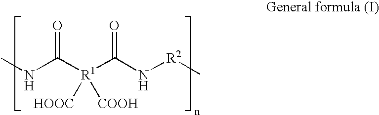
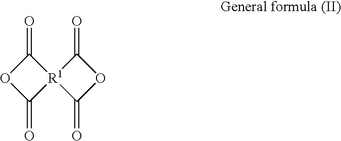
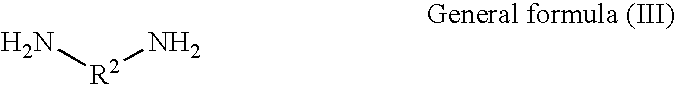
Method For Forming Surface Graft, Method For Forming Conductive Film, Method For Forming Method Pattern, Method For Forming Multilayer Wiring Board, Surface Graft Material, And Conductive Material
- Summary
- Abstract
- Description
- Claims
- Application Information
AI Technical Summary
Benefits of technology
Problems solved by technology
Method used
Image

Examples
example 1
(Synthesis of a Polyimide Precursor (Polyamic Acid))
[0227] 4,4′-diaminodiphenyl ether (5.75 g: 28.7 mmol) was dissolved in N-methyl pyrrolidone (30 ml) under nitrogen atmosphere, and the resultant solution was stirred for about 30 minutes at room temperature. To the solution, 3,3′,4,4″-benzophenonetetracarboxylic acid dianhydride (9.25 g: 28.7 mmol) was added at 0° C., and the resultant solution was stirred for 5 hours. The reaction solution was reprecipitated and a polyimide precursor was obtained. The molecular weight (Mw) measured by GPC was 28,000. The structure was observed by 1H-NMR and FT-IR.
(Preparation of a Polyimide Film)
[0228] Polyamic acid synthesized by the above technique was dissolved in DMAc (manufactured by Wako Pure Chemical Industries, Ltd.) to prepare a solution of 20 wt %. The solution was coated on a glass substrate by using a rod bar #36, and was dried at 100° C. for 5 minutes. The solution was then heated at 250° C. for 30 minutes to solidify the solutio...
example 2
[0240] The metal film formed in Example 1 was further electroplated for 15 minutes to produce a metal film 2.
Composition of an Electroplating Bath
[0241] Copper sulfate 38 g [0242] Sulfric acid 95 g [0243] Hydrochloric acid 1 mL [0244] Coppergreen PCM (manufactured by Meltex) 3 mL [0245] Water 500 mL
example 3
[0246] The polyimide substrate produced in Example 1 was immersed in a solution containing acrylic acid (10 wt %) and sodium periodate (NaIO4, 0.01 wt %) under an argon atmosphere. The above high-pressure mercury lamp of 1.5 kW was used, and the polyimide substrate was irradiated with light for 10 minutes. The obtained layer was sufficiently washed by ion exchanged water after the light irradiation, and the surface graft polymer of acrylic acid was introduced onto the whole substrate to produce a graft layer.
Adhesion of a Conductive Material
[0247] The graft layer produced above was immersed in a positive charge Ag dispersion solution (the conductive material is produced by the following technique). Then, the surface was sufficiently washed in flowing water, and the excessive Ag dispersing-solution was removed. A conductive film 2 (conductive material adhesion film) to which the conductive material was adhered was produced.
Manufacturing Method of a Conductive Material
[0248] Bis...
PUM
| Property | Measurement | Unit |
|---|---|---|
| Electrical conductivity | aaaaa | aaaaa |
| Electrical conductor | aaaaa | aaaaa |
| Energy | aaaaa | aaaaa |
Abstract
Description
Claims
Application Information
 - Generate Ideas
- Intellectual Property
- Life Sciences
- Materials
- Tech Scout
- Unparalleled Data Quality
- Higher Quality Content
- 60% Fewer Hallucinations
Browse by: Latest US Patents, China's latest patents, Technical Efficacy Thesaurus, Application Domain, Technology Topic, Popular Technical Reports.
© 2025 PatSnap. All rights reserved.Legal|Privacy policy|Modern Slavery Act Transparency Statement|Sitemap|About US| Contact US: help@patsnap.com