Liquid Logic Structures for Electronic Device Applications

a liquid logic and electronic device technology, applied in semiconductor devices, transistors, electrical devices, etc., can solve the problems of limited use of large-area electronics, limited use of low-cost substrates, and limitations on silicon wafer size, so as to increase the density, the effect of increasing the packing density

Active Publication Date: 2007-09-27
UNIVERSITY OF CINCINNATI
View PDF11 Cites 8 Cited by
  • Summary
  • Abstract
  • Description
  • Claims
  • Application Information

AI Technical Summary

Benefits of technology

[0007] In accordance with the principles of the invention, structures, devices and integrated circuits are provided with liquid logic. Liquid logic enables the fabrication of large area electronics (i.e., electronics on the human scale) such as flat panel displays, large array antennas, scanners / printers / copiers, large area sensors operating by chem / bio principles, thermal sensing, and radiation detection, full-size medical imaging systems, and photovoltaics. The liquid logic of the invention may be fabricated at room temperature, which permits the implementation of plastic substrates which are flexible and inexpensive and permits roll-to-roll processing. The liquid logic of the invention provides higher functionality by permitting the integration of various technologies / devices (i.e., hybrid electronics). The liquid logic of the invention increases packing density, which may permit fabrication of multi-layer or three-dimensional circuits of higher density than currently possible with conventional device technologies. The liquid logic of the invention is applicable to non-planar surfaces, unlike silicon-based technologies. For example, sensors may be formed using the liquid logic of the invention on curved surfaces of aircraft and spacecraft, soldiers, and other large-scale structures such as vehicles, power plants, bridges, etc. The liquid logic of the invention may also be applied to fabricate flexible electronics, such as electrotextiles (i.e., wearable electronics), electronic newspapers, and flexible large area displays and signs. The liquid logic devices of the invention utilize electric-field-controlled liquid components, which are distinguishable over devices in which liquid components are mechanically controlled, such as mercury switches.
[0008] The liquid logic devices of the invention are expected to exhibit superior electrical properties as compared with conventional alterative to silicon device technologies. Both n-channel and p-channel devices may be formed, which permits the creation of CMOS-like circuits that operate at low power. The carrier mobility is higher in the liquid logic devices of the invention than available in Organic FET's or amorphous silicon. The inventive liquid logic devices have a high current capability and are capable of bistable operation at low power. The inventive liquid logic devices are versatile in that CMOS-like transistors may be applied to many diverse applications. The inventive liquid logic devices may be formed by simple, room temperature fabrication techniques at a very low cost and using plastic substrates. The inventive liquid logic devices may be fabricated by non-lithographic wet / soft processing methods, such as ink jet printing, molding, and stamping, and may be formed by roll-to-roll fabrication techniques. The inventive liquid logic may be easily integrated with micro- and macro-fluidic applications.
[0009] The liquid logic and electrowetting switching of the invention may be applied to fabricate various device types, including but not limited to latches, transistors and inverters. Transistors may be formed with either upright or inverted component arrangements and as either p-channel or n-channel devices, which are easily and conveniently integrated on a single substrate.

Problems solved by technology

However, silicon based technologies face certain limitations.
Limitations on silicon wafer size limit use in large area electronics.
The high temperature processing required during silicon device processing prevents the use of low-cost substrates, such as plastics, and limits the application of advanced fabrication technologies, such as roll-to-roll processing.
Silicon-based electronics are difficult to integrate seamlessly with chemical / biological components.
Silicon device structures are fundamentally planar and are therefore difficult, if not impossible, to adapt to non-planar surfaces.
One alternative, quantum computing, has limited applications and has encountered manufacturing difficulties.
Another alternative, DNA computing, is time consuming and suffers from imprecise operation.
Yet another alternative, microfluidic computing, has found only limited applications.
Still another alternative, organic electronics, offers limited performance, lifetime and reliability.

Method used


Image

  • Liquid Logic Structures for Electronic Device Applications
  • Liquid Logic Structures for Electronic Device Applications
  • Liquid Logic Structures for Electronic Device Applications

Examples


example

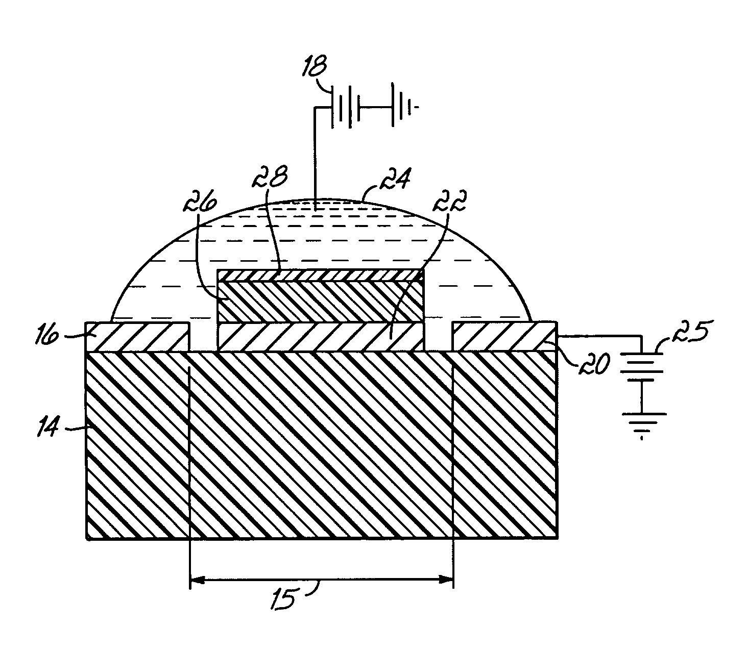
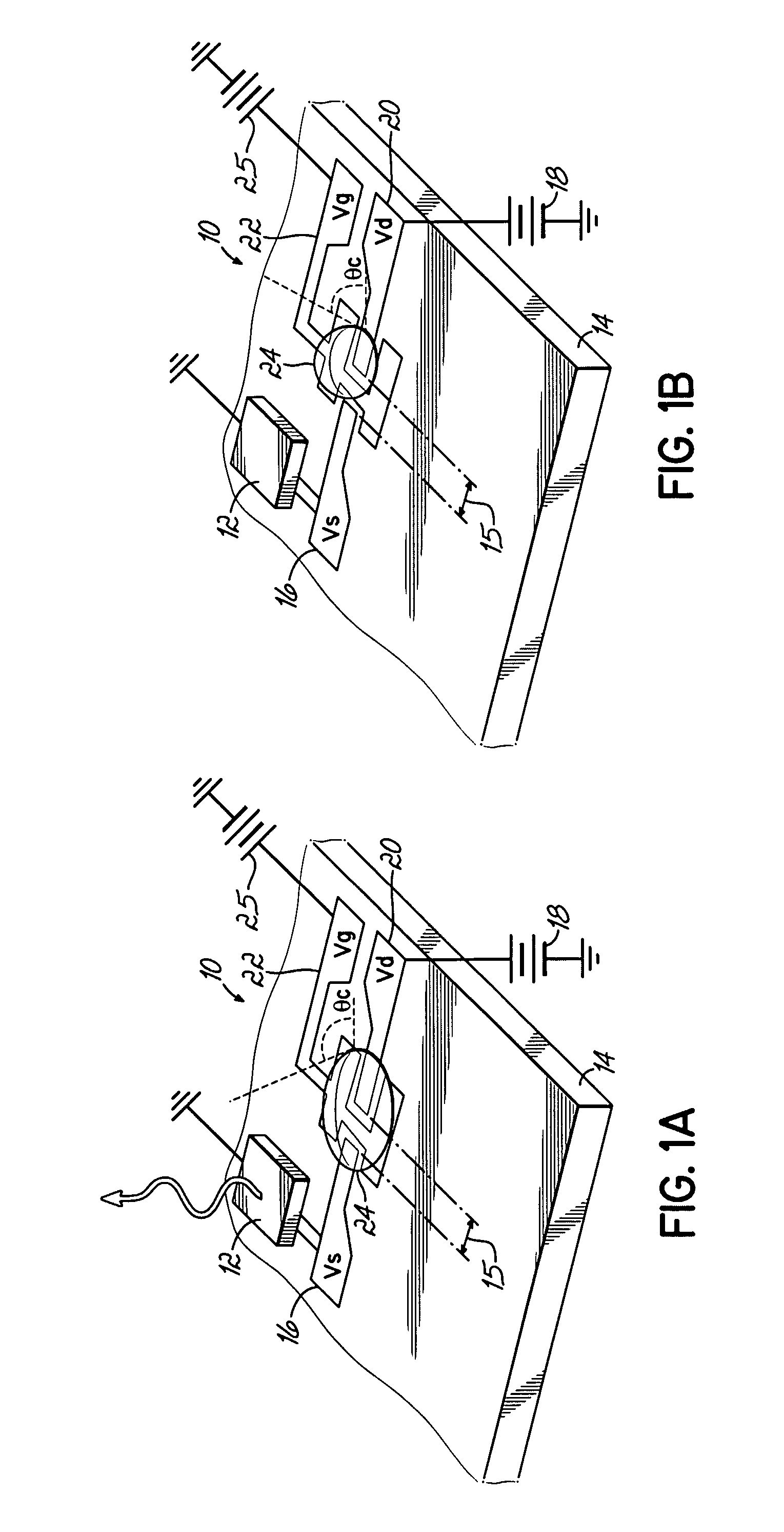
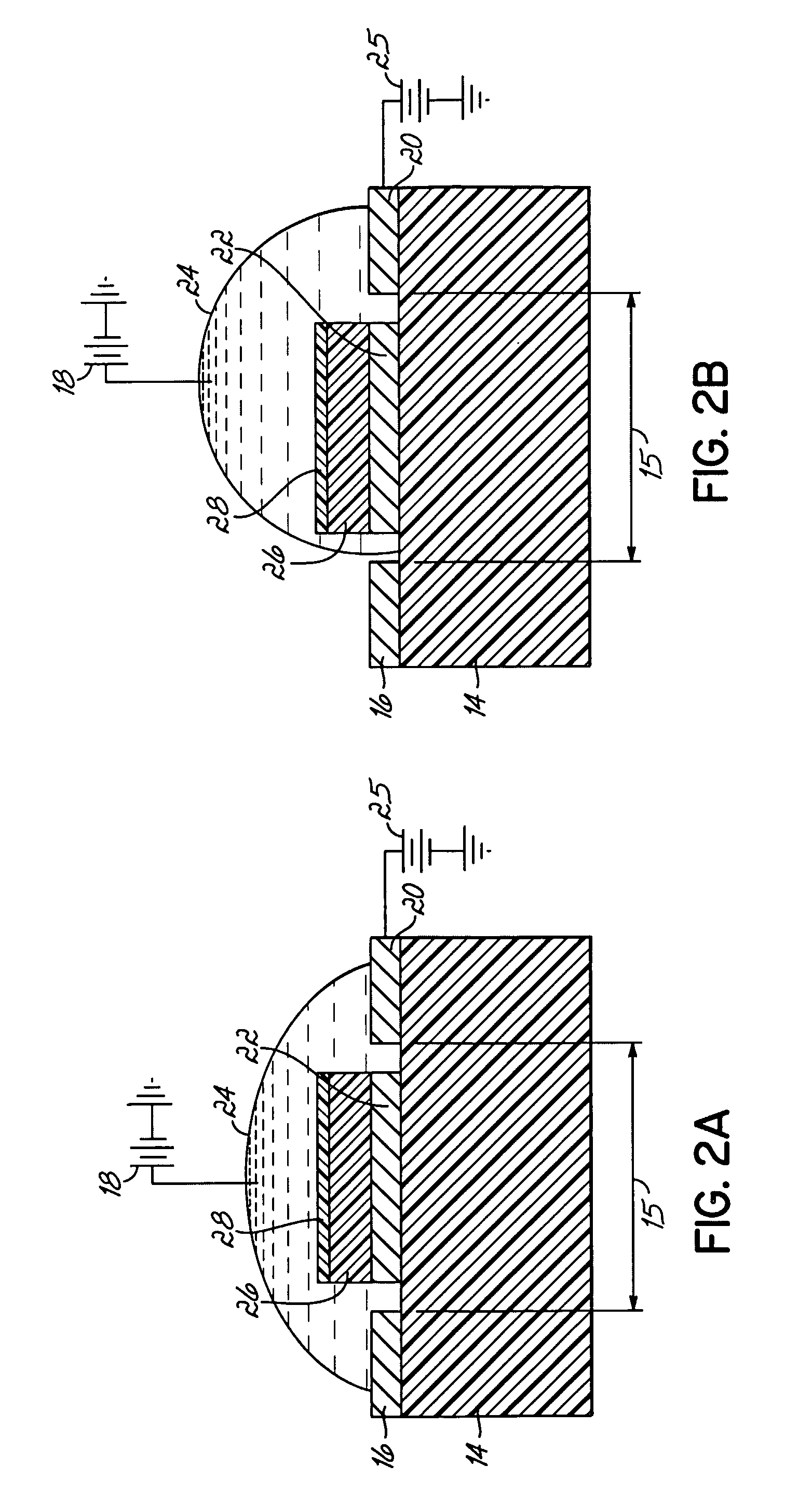
[0038] The prototype liquid logic device described in the example is most consistent with the device operation outlined in FIGS. 1A,B. A 3″ Si wafer was coated with an electrically insulating and hydrophobic DuPont Teflon AF fluoropolymer coating. An electrically conductive droplet containing water and PEDOT / PSS aqueous conductive polymer was then placed on the wafer. A drain electrode was inserted into the droplet, and a source electrode was placed adjacent to the droplet. The source and drain electrodes were then attached to an external battery and a functional device (LED) circuit. A gate electrode was attached to the upper surface of the droplet and a variable voltage source attached to the droplet with reference to the wafer (which acted as ground).

[0039] Upon application of an appropriate gate voltage (10V to 40V) to the droplet, the droplet wetted the hydrophobic surface of the wafer. This decreased the contact angle of the droplet to the hydrophobic surface and caused the d...


PUM


Abstract

Electronic devices (10, 30, 50) utilizing electrically-controlled liquid components to accomplish device switching. Electric fields are used in a device structure to manipulate the position and/or geometrical shape of a conductive fluid or liquid (60, 24) using electrowetting. This manipulation regulates the flow of current between electrodes of the device structure, such as the source and drain regions (16, 20) of a transistor construction, by bridging a non-conductive channel (15) separating the electrodes (16, 20) so that the electrodes (16, 20) are electrically coupled.

Description

CROSS-REFERENCE TO RELATED APPLICATIONS [0001] This application claims the benefit of U.S. Provisional Application No. 60 / 573,662, filed on May 21, 2004, the disclosure of which is hereby incorporated by reference herein in its entirety.FIELD OF THE INVENTION [0002] The invention relates generally to semiconductor structures and devices and, more particularly, to structures, devices, and integrated circuits utilizing liquid logic and methods of fabricating such structures, devices, and integrated circuits. BACKGROUND OF THE INVENTION [0003] Semiconductor devices, such as field effect transistors (FET's), are familiar building blocks of integrated circuits formed in silicon substrates. A single silicon-based integrated circuit may feature many thousands to millions of FET's, along with other passive components such as resistors and capacitors. However, silicon based technologies face certain limitations. Limitations on silicon wafer size limit use in large area electronics. The high ...

Claims


Application Information

Patent Timeline
Patent Type & Authority Applications(United States)
IPC IPC(8): H01H29/06H01H59/00H01L29/66H01L29/72
CPCH01H2029/008H01H59/0009
Inventor STECKL, ANDREW J.HEIKENFELD, JASON C.
Owner UNIVERSITY OF CINCINNATI
Why Eureka
Try Eureka