

Method and manufacturing low leakage MOSFETs and FinFETs
a technology of mosfets and finfets, which is applied in the field of fabricating field effect transistors (fets), can solve the problems of several problems of conventional mosfets, reduce stress propagation/relief, reduce defects as well as leakage and parasitic currents, and reduce leakage currents
- Summary
- Abstract
- Description
- Claims
- Application Information
AI Technical Summary
Benefits of technology
Problems solved by technology
Method used
Image

Examples
Embodiment Construction
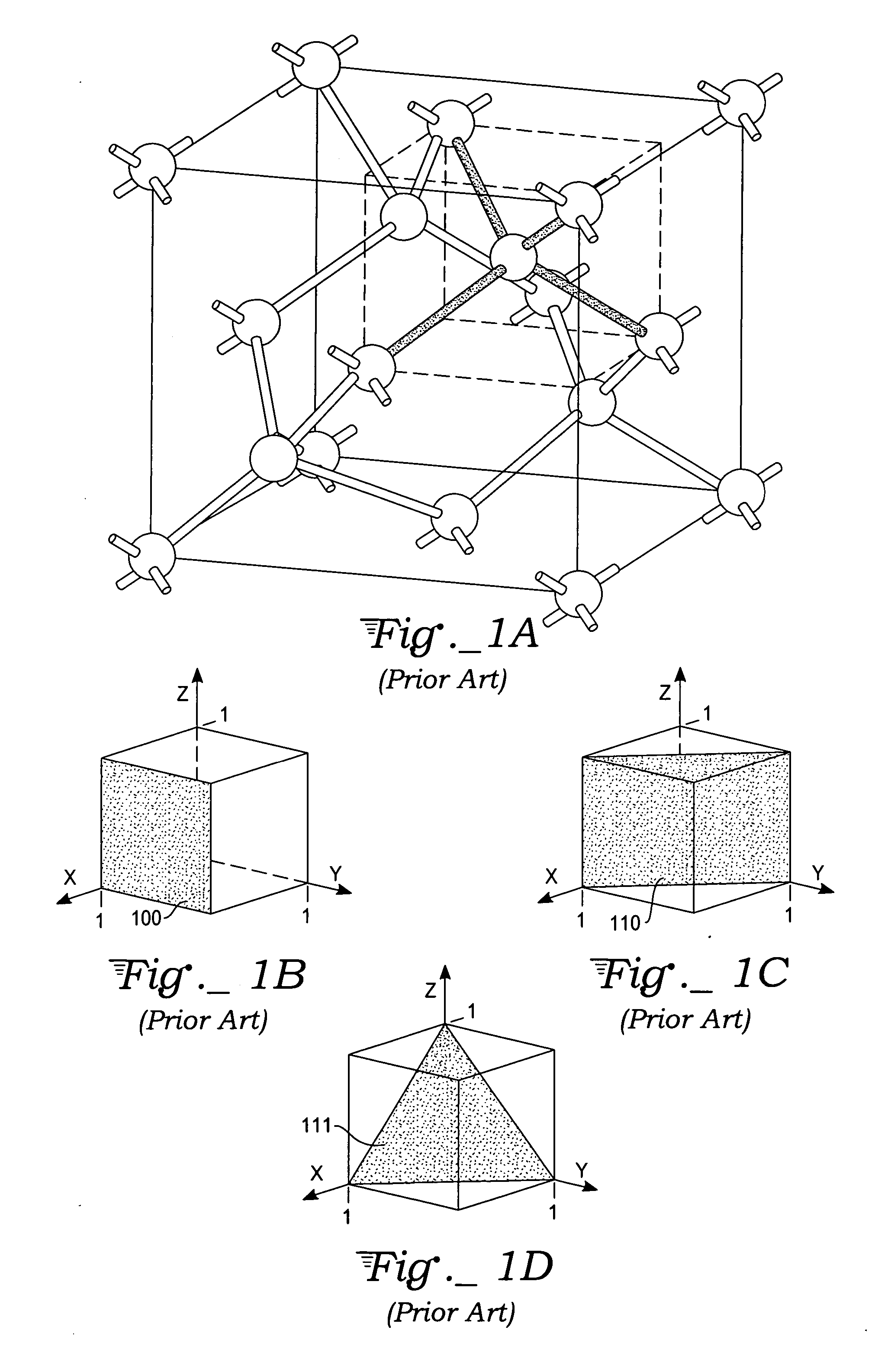
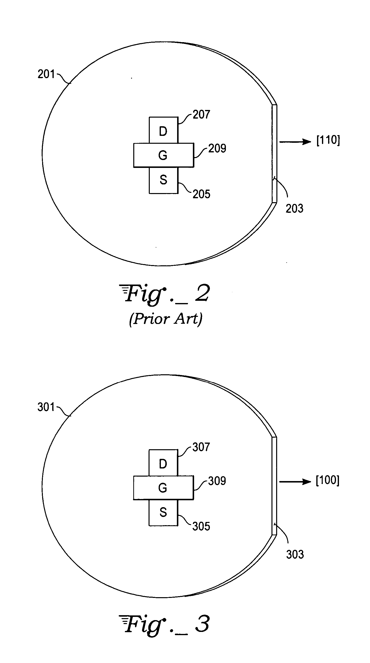
[0020] As device dimensions continue to shrink and thermal cycling continues to increase due to an increase in fabrication steps, defects (e.g., crystalline, contamination, etc.) have a more significant impact on device yield and performance. By aligning the primary flat (or notch) of, for example, an epi wafer with the (100) plane rather than the (110) plane, devices can be formed with traditional fabrication equipment wherein primary currents flow along the (100) plane rather than the (110) plane. In FIG. 3, an epi wafer 301, is shown with a single MOSFET device, including a source 305, a drain 307, and a gate 309 wherein a source-drain current channel is aligned to a primary flat 303. The primary flat 303 is aligned with the (100) plane. Fabricating devices with a primary current path aligned with the (100) plane reduces defects in and parallel to primary current paths and consequently reduces leakage and parasitic currents, as well as increases device yields.
[0021] An exemplary...
PUM
 Abstract
Description
Claims
Application Information