Substrate processing method and apparatus

a processing method and substrate technology, applied in the field of substrate processing methods and apparatuses, can solve the problems of low reliability, slow film formation speed, and low productivity of filling holes with a size on the order of several ten m, and achieve the effects of reducing manufacturing costs of semiconductor devices, processing time, and high reliability of semiconductor devices

Inactive Publication Date: 2007-11-01
EBARA CORP
View PDF9 Cites 16 Cited by
  • Summary
  • Abstract
  • Description
  • Claims
  • Application Information

AI Technical Summary

Benefits of technology

[0036]According to the present invention, the processing time when a hole having a diameter of several ten μm formed in a substrate is filled by a plating method can be shortened greatly, manufacturing cost of a semiconductor device can be reduced, and high reliability of the semiconductor device can be achieved.

Problems solved by technology

In these methods, the CVD method and the PVD method require a large-scale apparatus, and have disadvantages that the film formation speed is slow and productivity of filling a hole having a size on the order of several ten μm is low.
The reflow method is performed by a simple apparatus, but has disadvantages that material is melted by reheating to cause deterioration of the material, local corrosion is caused by contact between interconnect material on the chip and different metal having a low melting point to lower reliability, and resistance becomes high due to formation of intermetalic compounds.
Therefore, a large-scale plating apparatus is required to ensure throughput capacity of the process, and a number of plating cells are required so as to cope with parallel processing, thus increasing manufacturing cost of the semiconductor device.

Method used


Image

  • Substrate processing method and apparatus
  • Substrate processing method and apparatus
  • Substrate processing method and apparatus

Examples


example 1

Example of the First Invention

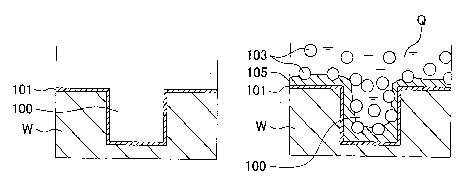
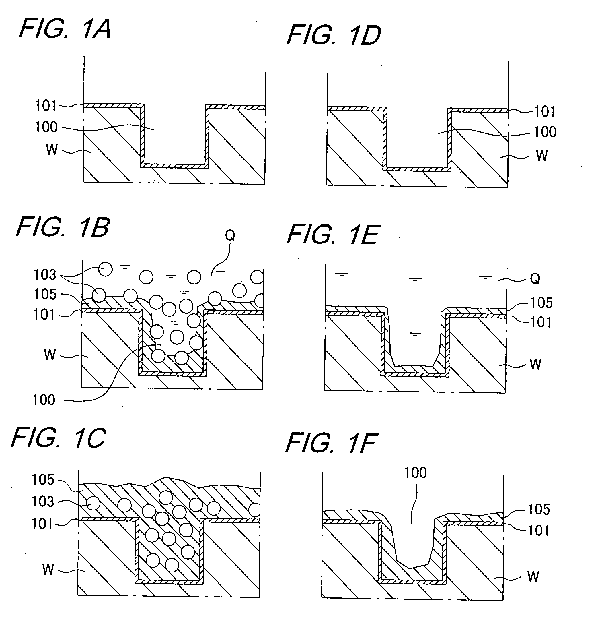
[0099]A basic plating bath was prepared by adding additives to a copper plating solution, for semiconductor backend process, composed mainly of copper sulfate. Hexadecyltrimethylammonium chloride was used as cationic surfactant, and PTFE powder (Fluon PTFE manufactured by Asahi Glass Co., Ltd.) was used as filler, thus making up a plating solution. The concentration of PTFE powder was 20 g / L, and the concentration of the surfactant was determined based on the surface tension of the plating solution. A substrate having a copper film formed on a Si substrate by a sputtering method was used, and a SUS plate was used as a counter electrode. The plating was carried out using a plating solution containing the filler and using a plating solution (basic plating bath) containing no filler, respectively by a constant current method in which current value and plating time were fixed. The thicknesses of the films on the specimens after plating were measured using a...

example 2

Eample of the Second Invention

(1) Example of Precipitation by Gravity of Filler

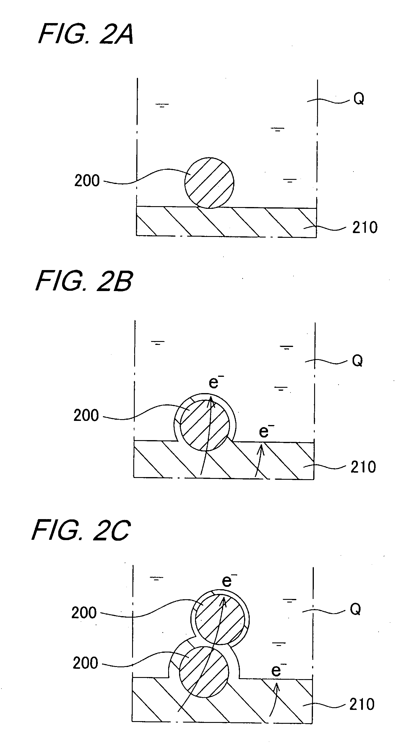
[0101]A basic plating bath was prepared by adding additives to a copper plating solution, for semiconductor backend process, composed mainly of copper sulfate. Hexadecyltrimethylammonium chloride was used as cationic surfactant, and PTFE powder (Fluon PTFE manufactured by Asahi Glass Co., Ltd. (particle diameter is equal to about 1 μm)) was used as filler, thus making up a plating solution. The concentration of PTFE powder was 20 g / L, and the concentration of the surfactant was determined based on the surface tension of the plating solution. A substrate having a copper film formed on a Si substrate by a sputtering method was used, and a SUS plate was used as a counter electrode. The plating was carried out using a plating solution containing the filler by a constant current method in which current value and plating time were fixed. The direction of the substrate was two directions of vertical and face up...


PUM

PropertyMeasurementUnit
sizeaaaaaaaaaa
sizeaaaaaaaaaa
diameteraaaaaaaaaa

Abstract

A substrate processing method is useful for filling a hole formed in a substrate with conductive material. The substrate processing method includes forming a non-through hole in a substrate, and filling the non-through hole with conductive material by plating. The plating is performed using a plating solution containing solid particles.

Description

BACKGROUND OF THE INVENTION[0001]1. Field of the Invention[0002]The present invention relates to a substrate processing method and apparatus, and more particularly to a substrate processing method and apparatus useful for filling holes formed in a substrate with conductive material. The present invention also relates to a semiconductor device processed by such substrate processing method.[0003]2. Description of the Related Art[0004]As electronic equipment has become smaller equipment, higher processing speed, and lower power consumption in recent years, there has been a growing demand for high density connection between a semiconductor chip serving as a semiconductor device and a substrate or between the semiconductor chips. The semiconductor chip is hereinafter referred to as chip. Conventionally, a lead frame has been used for electrical connection between the chip and the substrate, and a wire bonding method for connecting a lead frame and a bonding pad on the chip by a gold wire...

Claims


Application Information

Patent Timeline
Patent Type & Authority Applications(United States)
IPC IPC(8): H05K3/36
CPCC25D7/04Y10T29/49156C25D15/02H01L21/2885H01L21/7684H01L21/76877H05K3/421H05K3/423H05K2201/0209H05K2201/0212C25D7/123C25D17/001Y10T29/49126Y10T29/49165Y10T29/49155C25D15/00
Inventor SUSAKI, AKIRANAKADA, TSUTOMU
Owner EBARA CORP
Why Eureka
Try Eureka