Plasma etch process using polymerizing etch gases across a wafer surface and additional polymer managing or controlling gases in independently fed gas zones with time and spatial modulation of gas content

a technology of etching gas and wafer surface, applied in the direction of fluid pressure measurement, instruments, vacuum gauges, etc., can solve the problems of etch stop or taper profile unavoidable, low center etch rate, and worsening etch rate or etch profile non-uniformity, so as to reduce etch stop and increase etch rate, the effect of slowing down the polymer deposition ra

Active Publication Date: 2007-11-01
APPLIED MATERIALS INC
View PDF35 Cites 57 Cited by
  • Summary
  • Abstract
  • Description
  • Claims
  • Application Information

AI Technical Summary

Benefits of technology

[0006] A plasma etch process etches high aspect ratio openings in a dielectric film on a workpiece in a reactor having a ceiling electrode overlying the workpiece and an electrostatic chuck supporting the workpiece. The process includes injecting a polymerizing etch process gas through an annular zone of gas injection orifices in the ceiling electrode, and evacuating gas from the reactor through a pumping annulus surrounding an edge of the workpiece. The high aspect ratio openings are etched in the dielectric film with etch species derived from the etch process gas while depositing a polymer derived from the etch process gas onto the workpiece, by generating a plasma in the reactor by applying VHF source power and/or HF and/or LF bias power to the electrodes at the ceiling and/or the electrostatic chuck. The process further includes slowing the deposition rate of the polym

Problems solved by technology

Such a center low etch rate, etch stop or taper profile has appeared to be unavoidable for a number of reasons.
These problems are exacerbated when attempting to increase the etch rate or improve profile by the expedient of increasing the process gas flow rate into the reactor chamber.
Such an increase in gas flow rate does not solve the problem of non-uniform residency time radial distribution across the wafer surface (and hence the non-uniform dissociation across the wafer surface), and may even worsen the problem, thereby worsening the etch rate or etch profile non-uniformity.
However, such a technique would further decrease the gas residency time (and dissociation) over the wafer center relative to the periphery, further worsening the etch rate or etch profile non-uniformity.
Thus, there appears to be no solution to the problem.
We have found that the problem arises with great severity when using particular combinations of fluorocarbon or hydrocarbon etch proce

Method used


Image

  • Plasma etch process using polymerizing etch gases across a wafer surface and additional polymer managing or controlling gases in independently fed gas zones with time and spatial modulation of gas content
  • Plasma etch process using polymerizing etch gases across a wafer surface and additional polymer managing or controlling gases in independently fed gas zones with time and spatial modulation of gas content
  • Plasma etch process using polymerizing etch gases across a wafer surface and additional polymer managing or controlling gases in independently fed gas zones with time and spatial modulation of gas content

Examples


Embodiment Construction

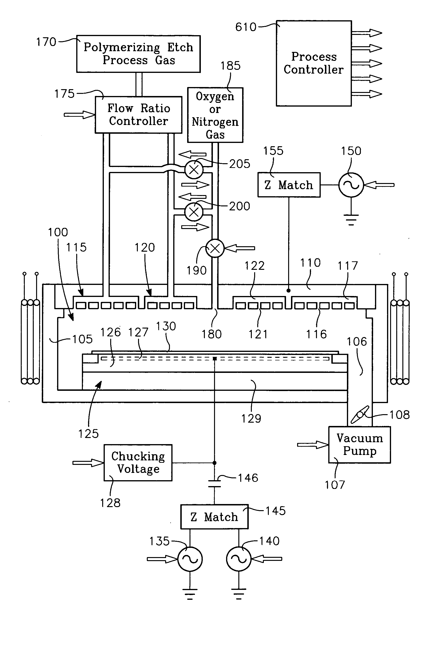
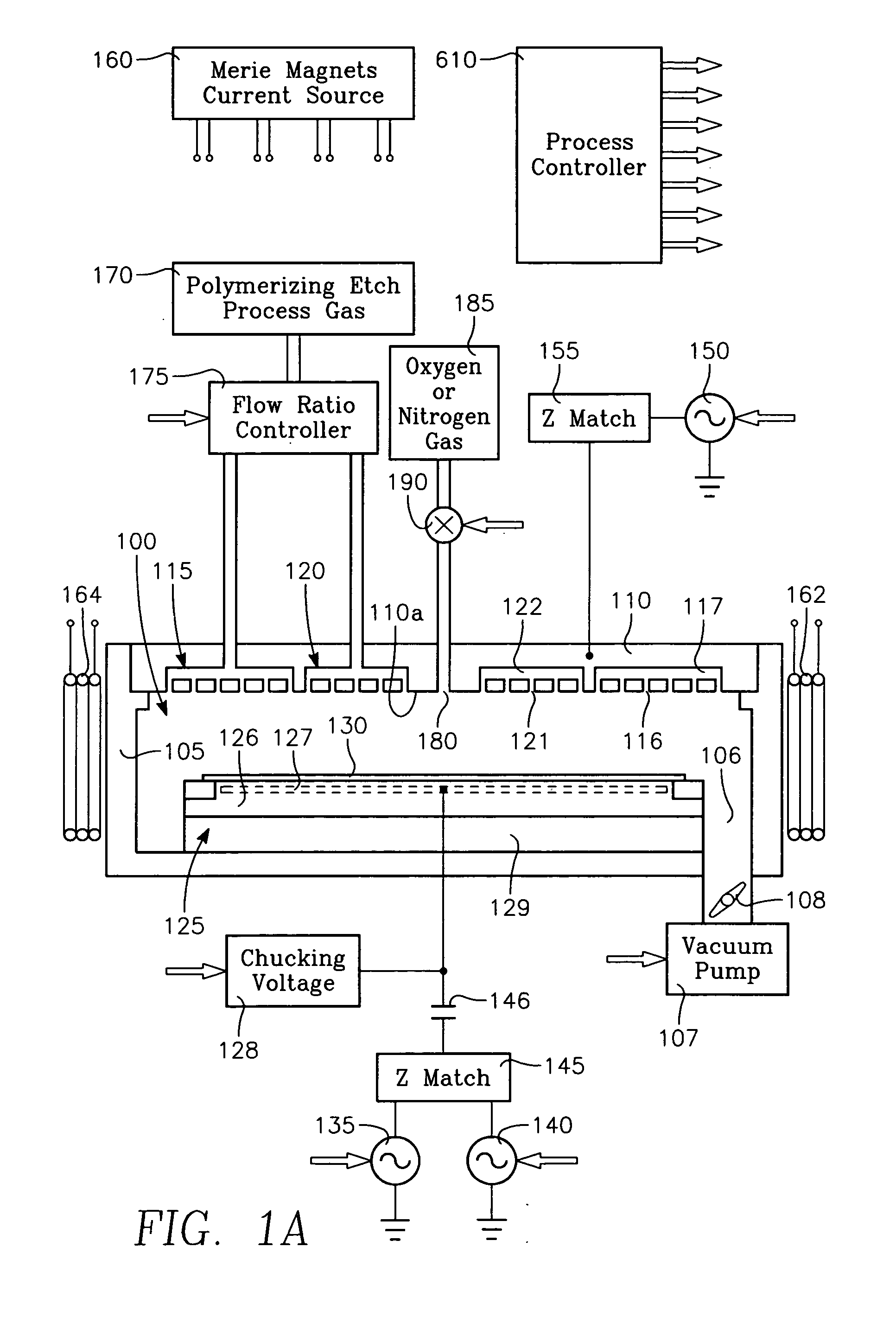
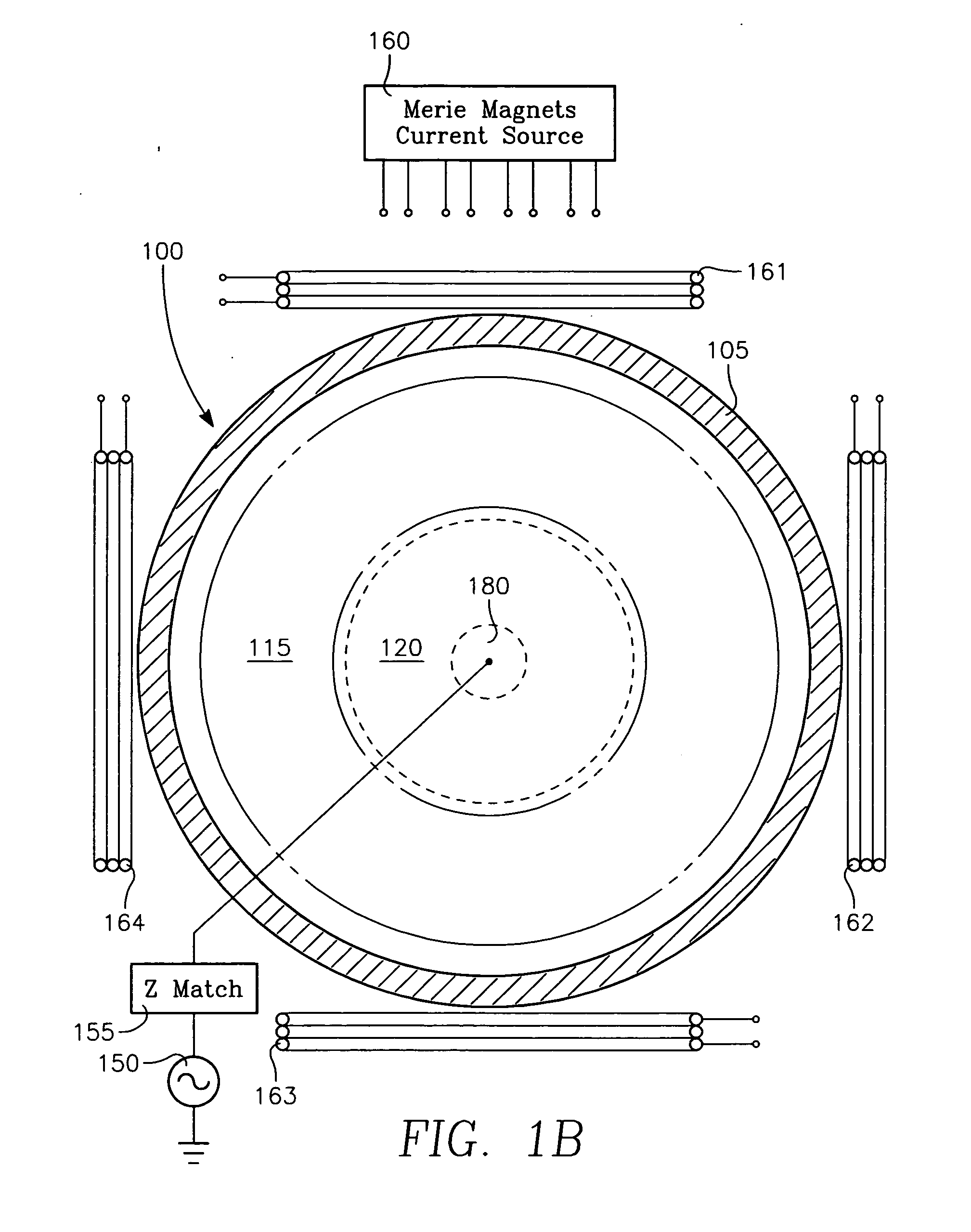
[0024] The present invention solves the problem of low etch rate in a region typically at the center of the wafer that has plagued capacitively coupled plasma etch processes for etching dielectric thin films. The invention is based upon our discovery that the problem can be completely solved without requiring any increase in etch process gas flow rate over the wafer center. It is further based upon our discovery that removing or slowing deposition of polymer on sidewalls and / or bottom of narrow openings at the wafer center during the etch process is an effective solution, rather than attempting to increase the etch gas flow rate at the wafer center. Finally, the invention is based upon our discovery that a gas such as oxygen or nitrogen which does not etch dielectric material, but which does remove polymer, is an essential part of this solution. The invention is realized by providing a novel independent gas injection orifice or zone, for example, at the center of the overhead electr...


PUM

PropertyMeasurementUnit
Flow rateaaaaaaaaaa
Ratioaaaaaaaaaa
Etch rateaaaaaaaaaa

Abstract

A plasma etch process etches high aspect ratio openings in a dielectric film on a workpiece in a reactor having a ceiling electrode overlying the workpiece and an electrostatic chuck supporting the workpiece. The process includes injecting a polymerizing etch process gas through an annular zone of gas injection orifices in the ceiling electrode, and evacuating gas from the reactor through a pumping annulus surrounding an edge of the workpiece. The high aspect ratio openings are etched in the dielectric film with etch species derived from the etch process gas while depositing a polymer derived from the etch process gas onto the workpiece, by generating a plasma in the reactor by applying VHF source power and/or HF and/or LF bias power to the electrodes at the ceiling and/or the electrostatic chuck. The process further includes slowing the deposition rate of the polymer, minimizing etch stop and/or increasing the etch rate in a region of the workpiece typically the center by injecting oxygen or nitrogen and/or high-fluorine containing gas through gas injection orifice in the corresponding region of the ceiling electrode, and adjusting the flow rate of the oxygen or nitrogen and/or high-fluorine containing gas through the gas injection orifice to minimize the difference between profiles and etch depths at the workpiece center and the workpiece periphery.

Description

BACKGROUND OF THE INVENTION [0001] Fabrication of integrated circuits with feature sizes on the order of nanometers requires etch processes that are extremely uniform across the entire surface of a semiconductor wafer, typically about 300 millimeters in diameter. Such uniform etch processes are typically realized in a plasma etch reactor such as a capacitively coupled plasma reactor with an overhead electrode having an extremely high aspect ratio (e.g., an electrode-to-wafer gap of only 2.5 cm for a 300 mm wafer). The etch process gas includes a gas of the type that forms a protective polymer layer over photoresist or other thin film surfaces that are not to be etched, such as a fluorocarbon gas or a fluorohydrocarbon gas. Formation of such a protective polymer layer enhances etch selectivity. [0002] Such processes exhibit a low etch rate, etch stop or taper profile at a region typically the center of the wafer and a high etch rate or bow profile at other region typically near the w...

Claims


Application Information

Patent Timeline
IPC IPC(8): C03C25/68C23F1/00
CPCH01J37/321H01L21/31116H01J2237/3347H01J37/32449
Inventor BERA, KALLOLZHAO, XIAOYEDOAN, KENNY L.GOLD, EZRA ROBERTBRILLHART, PAUL LUKASGEOFFRION, BRUNOPU, BRYANHOFFMAN, DANIEL J.
Owner APPLIED MATERIALS INC
Why Eureka
Try Eureka