Organic EL display device and organic thin film device

a display device and organic technology, applied in the direction of discharge tube luminescnet screens, natural mineral layered products, transportation and packaging, etc., can solve the problems of short life of the device, difficult so far to obtain an ink composition capable of stably discharging, and difficult to realize a high purity of organic materials as described previously, etc., to achieve the effect of viscosity

Inactive Publication Date: 2007-11-01
HITACHI DISPLAYS
View PDF1 Cites 10 Cited by
  • Summary
  • Abstract
  • Description
  • Claims
  • Application Information

AI Technical Summary

Benefits of technology

[0011] An object of the invention is to make it possible to manufacture an organic material of an organic EL display device to be configured of a low molecular weight organic material which can be subjected to distillation or sublimation purification by a wet method.
[0012] Another object of the invention is to make it possible to manufacture an organic material of an organic EL display device to be configured of a low molecular weight organic material which can be subjected to distillation or sublimation purification by a wet method.
[0013] In preparing an organic layer of an organic EL device of an organic EL display device by an inkjet method, there has hitherto been used an ink composition having a high molecular weight organic material dissolved in an aromatic solvent. FIG. 1 shows one example of a relationship between a boiling point and a viscosity of a solvent which is considered to be suitable for this ink composition and which is commercially available. As is clear from FIG. 1, a viscosity of the solvent suitable for the high molecular weight organic material is not more than 5mPa·s. In the case of a high molecular weight organic material, since when dissolved in a solvent, its viscosity may possibly increase several times, it is possible to obtain an optimum viscosity necessary for the ink discharge by inkjet even by using a solvent with low viscosity.
[0017] In the foregoing chemical formulae, A represents an alkyl group having not more than 4 carbon atoms. B represents chlorine or bromine. Also, D represents an electron-providing group and is a substituent selected among a dimethylamino group, a methoxy group, an ethoxy group, and a phenoxy group. Since this ink composition has a high boiling point, it has a characteristic feature that after drying, it remains more easily in a light emitting layer. Also, the aromatic compound of the invention has a characteristic feature that its hydrophobicity is higher than that of an organic material molecule of a light emitting material or the like to be dissolved.
[0018] Namely, in the case where an amorphous film is manufactured by using the foregoing ink composition, the compound represented by any one of the foregoing chemical formulae C1 to C6 can be made present in an organic material layer of an organic EL display device; and its organic material layer has high hydrophobicity and has an effect for inhibiting the penetration of a water molecule into an organic layer including a light emitting layer of an organic EL display device and is able to contribute to realization of a long life of an organic EL display device.

Problems solved by technology

Since Patent Document 1 is limited to a precursor of a conjugated high molecular weight organic compound (difficult in sublimation purification), it is difficult to realize a high purity of the organic material as described previously.
Thus, a life of the device was short.
Since a viscosity of a solvent for dissolving an organic material in light emitting devices or organic semiconductors is not more than 5 mPa·s, it was difficult so far to obtain an ink composition capable of stably discharging a low molecular weight organic material which can be subjected to distillation or sublimation purification by using an inkjet system with a droplet discharge capacity of 10 picoliters or more.

Method used


Image

  • Organic EL display device and organic thin film device
  • Organic EL display device and organic thin film device
  • Organic EL display device and organic thin film device

Examples


example 1

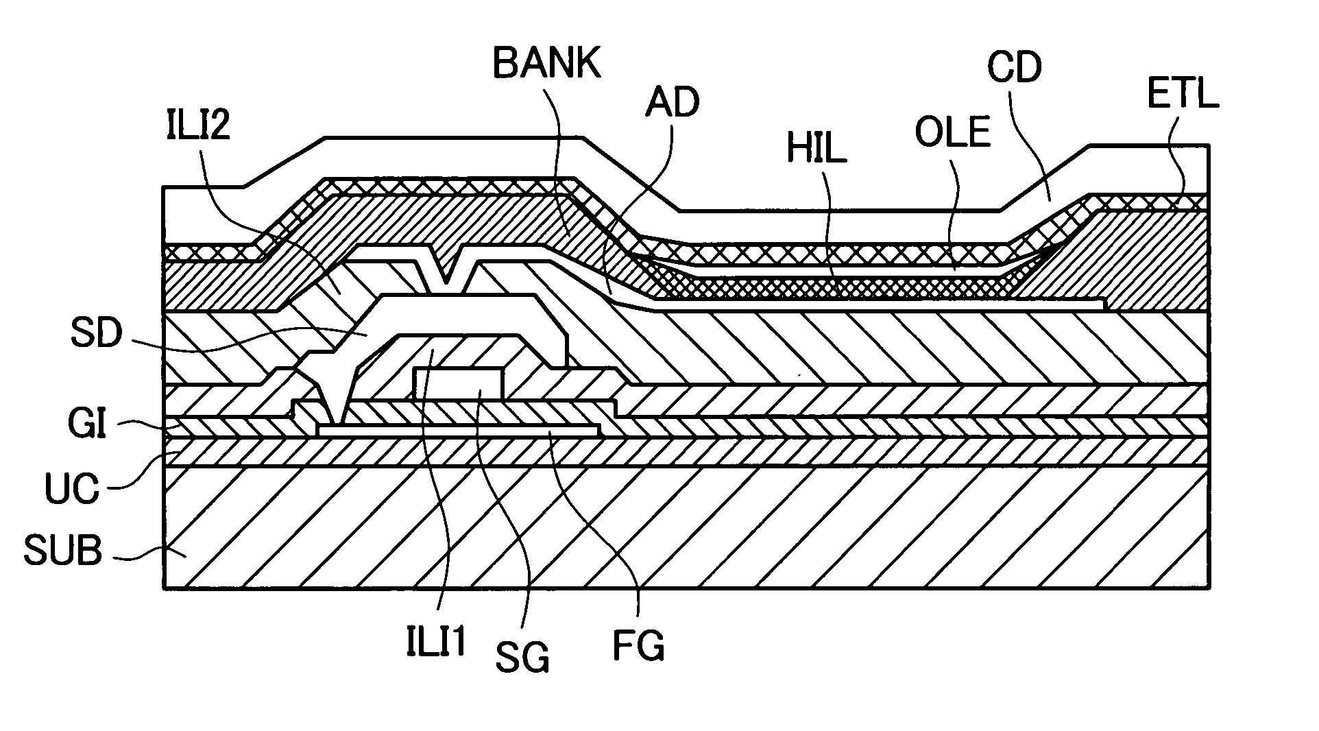
[0031]FIG. 3 shows a layer structure which is employed in the present Example. A structure in which a glass-made substrate SUB, an undercoat layer UC, a polysilicon layer FG, a gate insulating layer GI, a metallic gate electrode layer SG, a first interlayer insulating layer ILI1, a source·drain metallic layer SD, a second interlayer insulating layer ILI2, an EL device lower electrode layer AD, a bank BANK, an organic functional layer OEM (including a hole injection layer HIL, a light emitting layer OLE and an electron transport layer ETL), and an upper electrode CD are stacked in this order is provided on a first substrate. The substrate SUB is an alkali-free glass having a thickness of 1.1 mm. The undercoat layer UC is configured of a silicon nitride layer having a thickness of 150 nm and a silicon oxide layer having a thickness of 100 nm as formed by means of plasma CVD. The p-Si layer FG is formed in an island form in a forming place of a thin film transistor (hereinafter referre...

example 2

[0043] Au was vapor deposited in a thickness of 20 nm on a polyimide substrate having a thickness of 150 μm at a vapor deposition rate of 0.1 nm / sec under vacuum of 10−6Torr. This was subjected to patterning by a photolithography method, thereby forming a source-drain electrode. A source-to-drain channel length was set up at 10 μm.

[0044] Next, 1,3,5-tris[4-(diphenylamino)phenyl]-benzene (TDAPB, manufactured by Bayer AG) was dissolved in a 1 / 1 mixed solvent of 1,2,3-trimethoxybenzene and 3,4,5-trimethoxy-toluene so as to have a solids concentration of 0.5% by weight, and the solution was passed through a PTFE-made filter of 0.2 μm to form an organic semiconductor layer forming ink.

[0045] This ink was fabricated in a thickness of 50 nm on the hole injection layer within the pixel by using a piezoelectric type inkjet system and baked on a hot plate at 85° C. for 15 minutes, thereby obtaining an amorphous film.

[0046] Subsequently, an SiO2 film having a thickness of 500 nm was formed ...


PUM

PropertyMeasurementUnit
viscosityaaaaaaaaaa
viscosityaaaaaaaaaa
thicknessaaaaaaaaaa

Abstract

An object of the invention is to provide a manufacturing method of an organic EL display device by fabricating a low molecular weight light emitting material on a lower electrode of an organic EL display device by an inkjet method. In order to achieve this object, in an organic EL display device including an organic material layer, the organic material layer is configured of a mixture of a low molecular weight material and a specified organic material. Concretely, at least one compound selected from 1,2,3-trimethoxytoleune, 1,2,3, 5-tetramethoxybenzene, 1,2-dimethoxy-5-bromobenzene, 3,4-dimethoxy-6-bromotoluene, 1,2,3-trimethoxy-5-bromo-benzene, and 3-bromo-1,2-benzodioxane is contained.

Description

CROSS-REFERENCE TO RELATED APPLICATIONS [0001] The disclosure of Japanese Patent Application No. 2006-109357 filed on Apr. 12 2006 including the claims, the specification, the drawings and the abstract is incorporated herein by reference in its entirety. BACKGROUND OF THE INVENTION [0002] 1. Field of the Invention [0003] The invention relates to an organic thin film device. [0004] 2. Description of the Related Art [0005] An organic thin film device includes an organic EL display device and an organic thin film transistor. As a manufacturing method of an organic EL display device, there are known a method of fabricating a low molecular weight organic material by a vacuum vapor deposition method (vacuum vapor deposition method) and a method of fabricating a high molecular weight organic material by a wet method such as an inkjet method and a screen printing method. With respect to the vacuum vapor deposition method, since it is difficult to improve the registration of a mask, it is sa...

Claims


Application Information

Patent Timeline
Patent Type & Authority Applications(United States)
IPC IPC(8): H01L51/54H01L51/56
CPCH01L51/0007H01L51/0059H01L51/007H01L51/56H01L51/0085H01L51/0541H01L51/5012H01L51/0081Y10T428/31504H10K71/15H10K85/6565H10K85/631H10K85/324H10K10/464H10K85/342H10K50/11H10K71/00
Inventor UCHINO, SHOICHOIWATA, AKIKOARAI, YOSHIHIROYAGUCHI, TOMIO
Owner HITACHI DISPLAYS
Why Eureka
Try Eureka