Method of growing gallium nitride crystal and gallium nitride substrate
- Summary
- Abstract
- Description
- Claims
- Application Information
AI Technical Summary
Benefits of technology
Problems solved by technology
Method used
Image

Examples
embodiment 1
Dependence upon first growth temperature Te
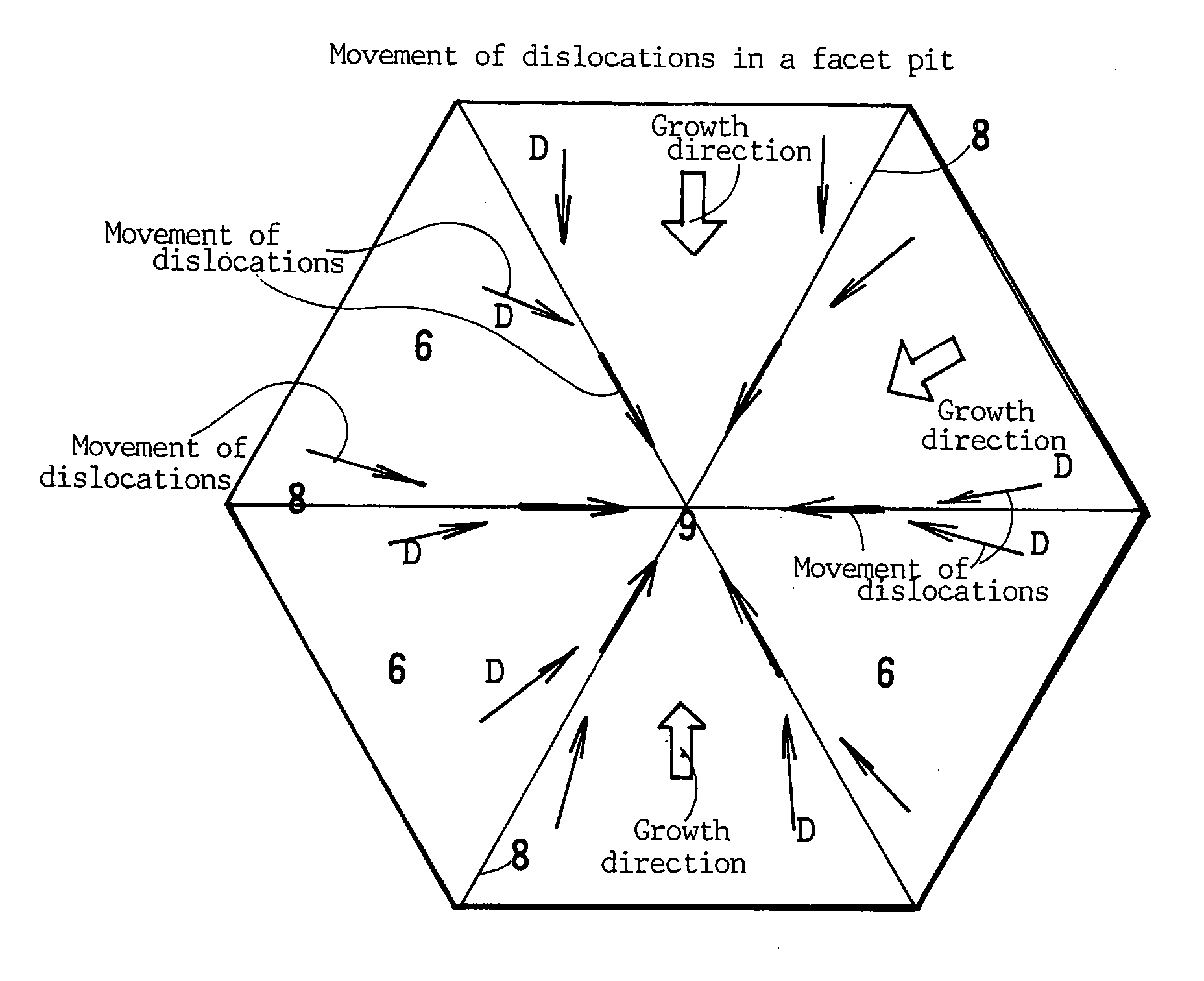
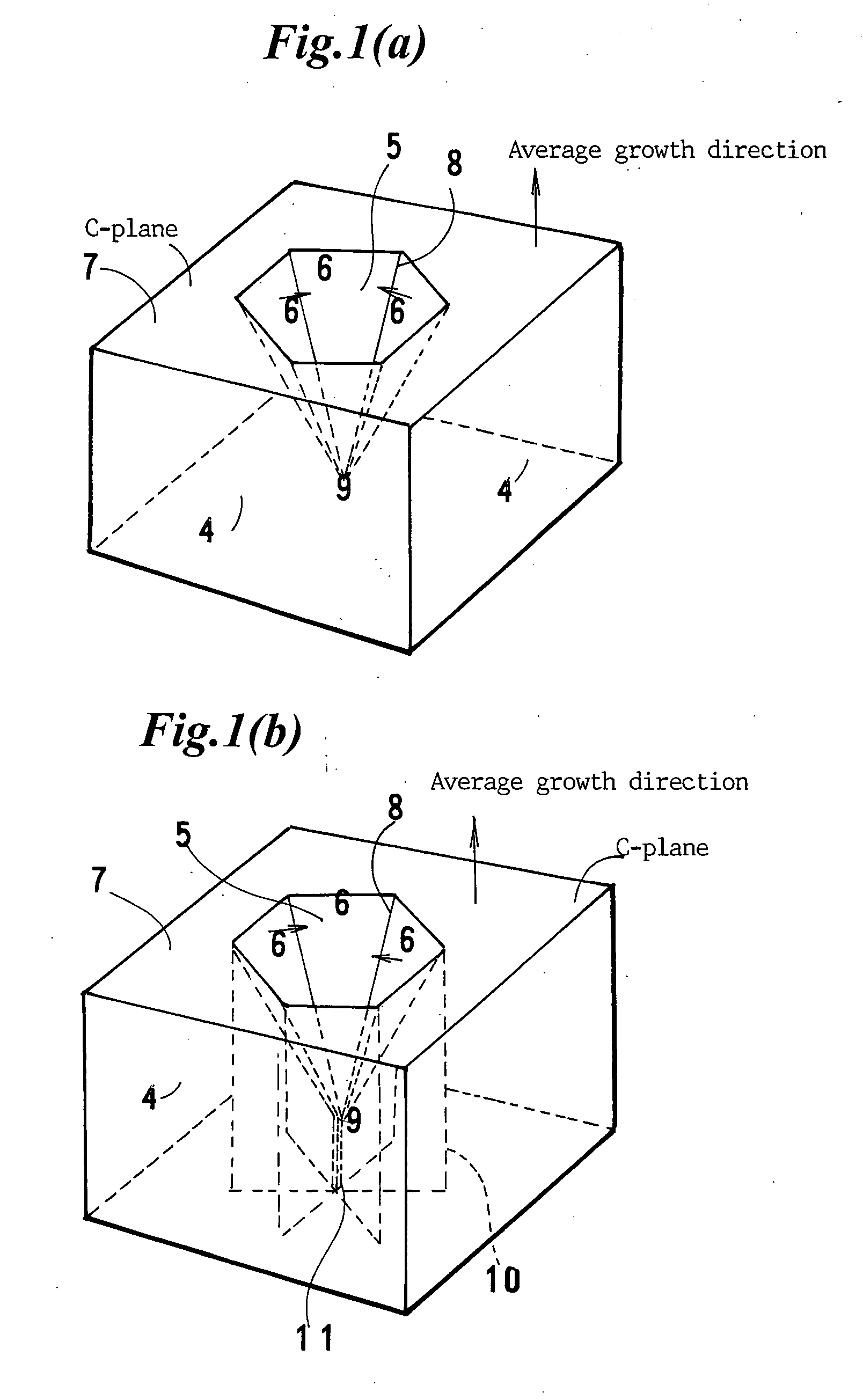
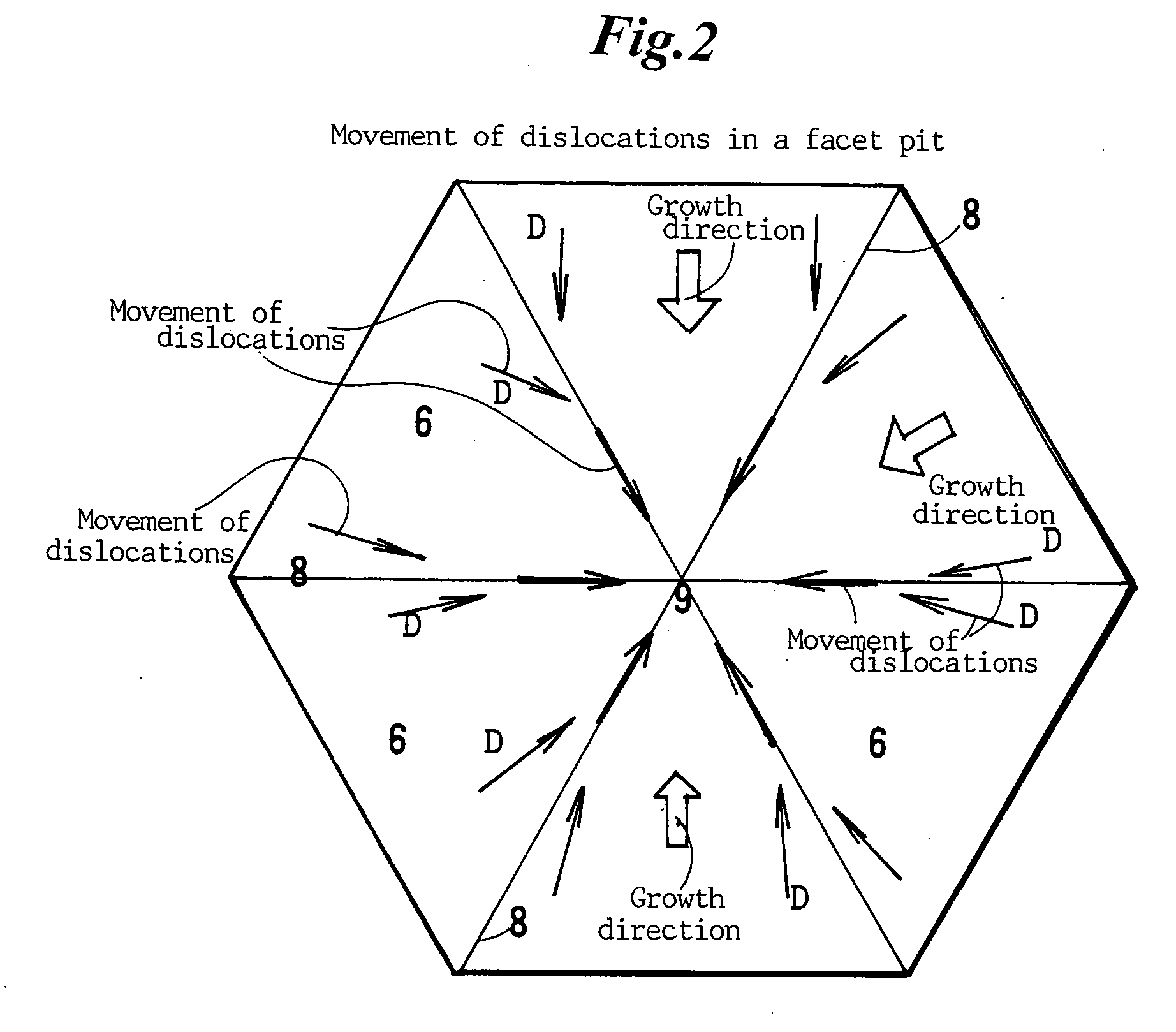
[1. Undersubstrate (U)]
[0089] Three kinds U1, U2 and U3 of undersubstrates are prepared. U1 is 2-inch diameter sapphire (Al2O3) single crystal substrates. U2 is 2-inch diameter gallium arsenide (GaAs) single crystal substrates. U3 is 2-inch diameter sapphire substrates covered with a 1.5 μm thick GaN epitaxially grown by an MOCVD method. The sapphire undersubstrates (U1) are C-plane (0001) surface wafers. The GaAs undersubstrates (U2) are (111)A-plane wafers. The GaN / sapphire undersubstrates (U3) have a mirror (0001) GaN surface. A GaN / sapphire wafer is sometimes called a “template”.
[2. Mask patterns (M)]
[0090] 0.1 μm thick SiO2 films are produced on the three kinds of undersubstrates U1, U2 and U3. Two kinds of patterns are formed by photolithography and etching. One is a stripe pattern (M1) having parallel mask stripes. The other is a dot pattern (M2) having isolated mask dots. The parts which are not covered with masks are named expos...
embodiment 2 (
Solid Carbon)
[0140] Embodiment 2 grows GaN crystals on SiO2 masked (M1 and M2) C-plane sapphire undersubstrates (U1), GaAs undersubstrates (U2) and GaN / sapphire undersubstrates in the same furnace as Embodiment 1 for 60 minutes with a supply of carbon. Embodiment 2 differs from Embodiment 1 in the method of carbon supply. Instead of supplying hydrocarbon gases, Embodiment 2 uses solid carbon. A carbon plate is placed at a higher temperature part set at an upstream of the growth part (susceptor) in the HVPE furnace. The other conditions are similar to Embodiment 1.
[0141] Undersubstrates (U1, U2 and U3) with stripe and dot masks (M1; M2) are put on the susceptor in the furnace.
[0142] At an early stage, GaN buffer layers are grown for 15 minutes on the M1, M2-masked undersubstrates (U1, U2 and U3) at a low temperature of about 500° C. (Tb=500° C.) under an ammonia partial pressure PNH3=0.2 atm (20 kPa) and a PHCl partial pressure PHCl=2×10⁻³ atm (0.2 kPa). The thickness of the GaN bu...
PUM
 Abstract
Description
Claims
Application Information