Semiconductor device including cmis transistor

a technology of cmis transistor and semiconductor device, which is applied in the direction of transistors, semiconductor devices, electrical appliances, etc., can solve the problems of not being able to achieve normal operation of the semiconductor device, unable to manufacture the cmos device, and unable to achieve expected drain curren

Inactive Publication Date: 2007-12-13
RENESAS TECH CORP
View PDF1 Cites 39 Cited by
  • Summary
  • Abstract
  • Description
  • Claims
  • Application Information

AI Technical Summary

Benefits of technology

[0024]It is an object of the present invention to provide, taking aforementioned problems into consideration, both when forming the dual gates with metal silicides different from each other and when forming the dual gates with metal and metal alloy, a method of preventing mutual diffusion of said metal film atoms (gate materials) in forming gate electrodes.

Problems solved by technology

However, the method of forming a microscopic gate electrode and forming the CMOS transistor is described as only “Lift-off” in “table 1”, and a specific method is not proposed, and thus is difficult to actually manufacture the CMOS device, and an effective method is not disclosed for the method of forming the dual gate when using metal for the gate material different from the case of the metal silicide.
That is, in the vicinity of the PN isolation, the threshold voltage of the transistor fluctuates when deviated from the desired metal silicide material or composition and the work function changes, and the expected drain current may not be obtained.
As a result, the normal operation of the semiconductor device cannot be obtained, and the yield lowers.
“Tunable Work Function Dual Metal Gate Technology for Bulk and Non-Bulk CMOS”, IEEE IEDM 2002, specific method of forming the gate electrode is not proposed, and a problem in that the transistor performance changes due to mutual diffusion similarly arises when using different metal alloys as in JaeHoon Lee et al.

Method used


Image

  • Semiconductor device including cmis transistor
  • Semiconductor device including cmis transistor
  • Semiconductor device including cmis transistor

Examples


first embodiment

Effect of First Embodiment

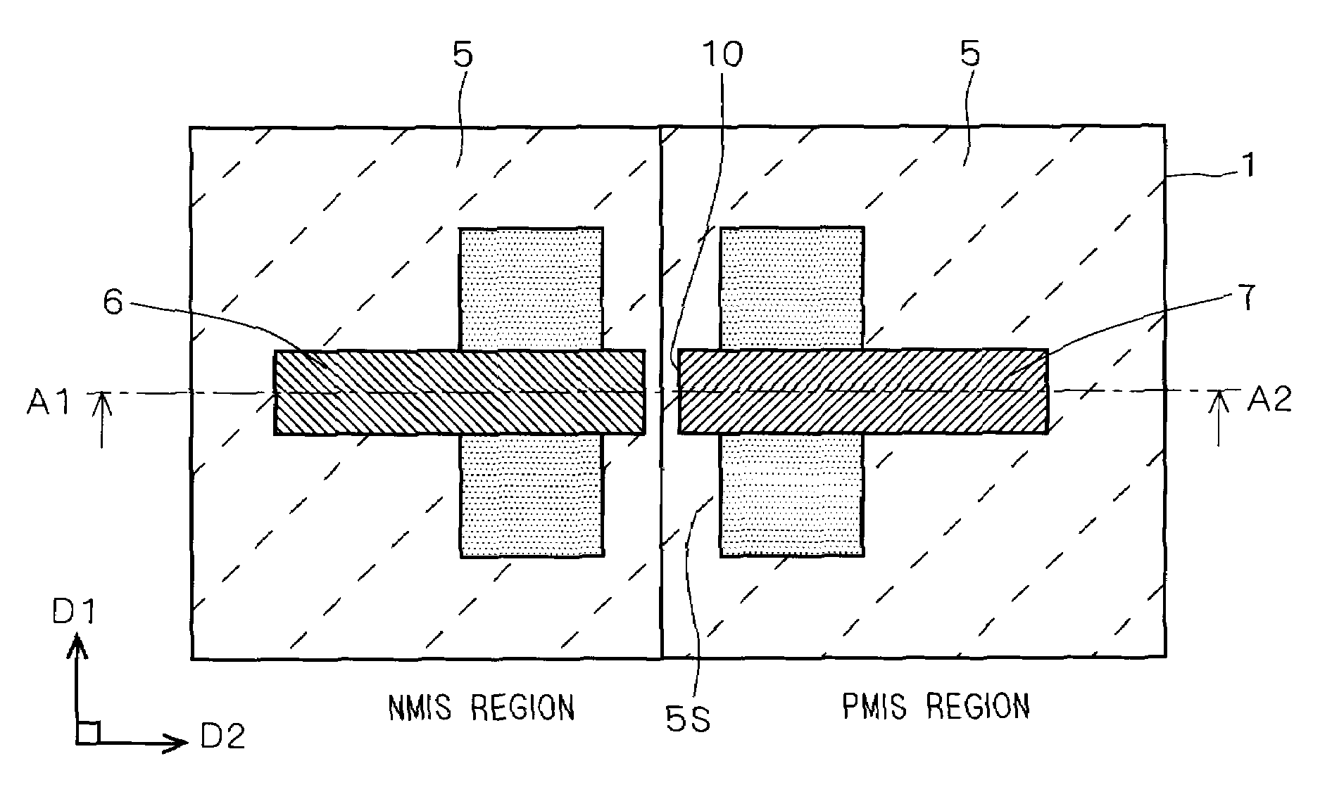
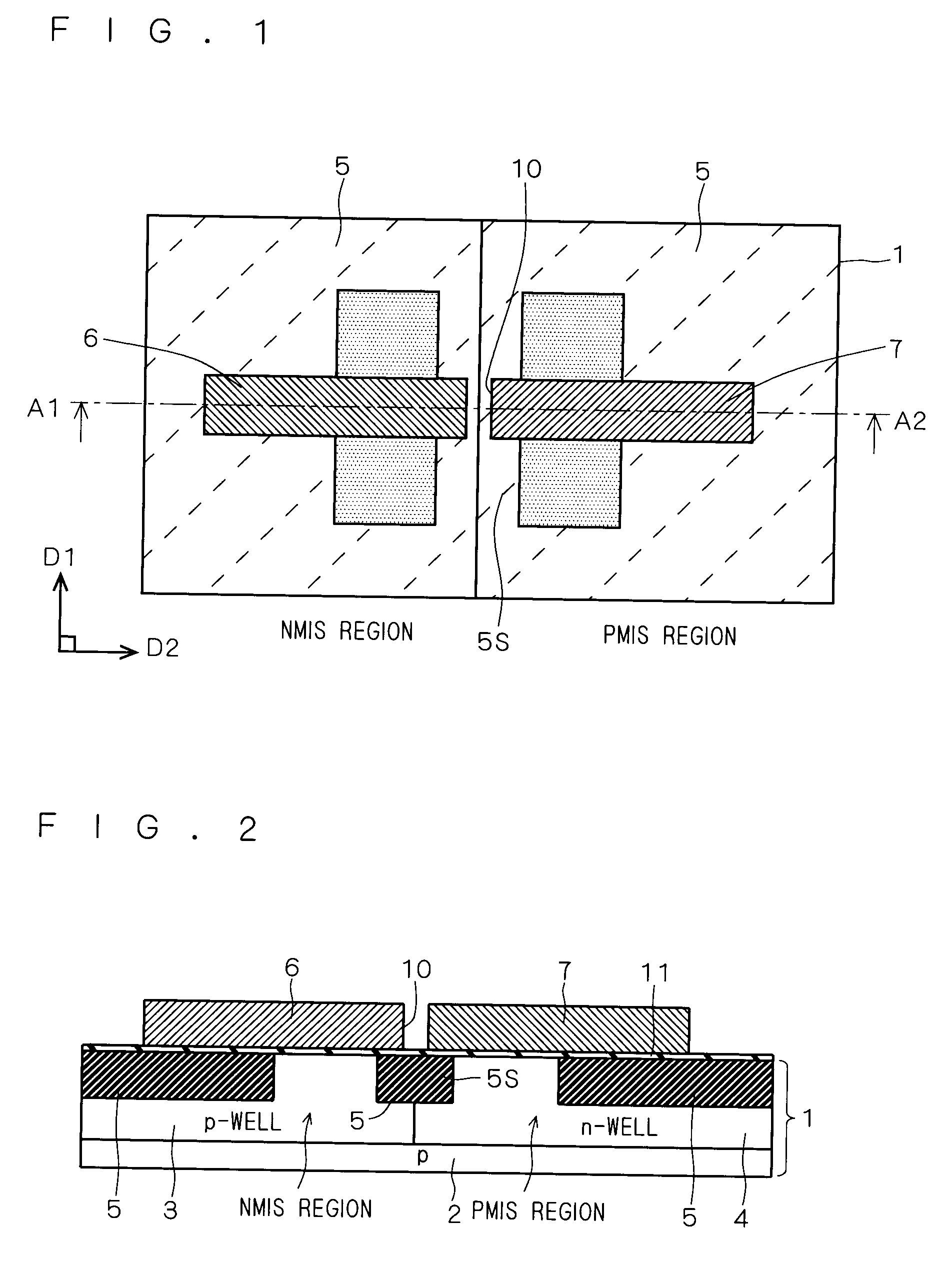
[0066]In the present embodiment, the pattern of the gate electrodes is assumed to have an independent shape for the NMIS region and the PMIS region, and the connection between the gates at the PN boundary is realized with the conducive film 20 to be filled into the connection hole 19 formed in the inter-layer insulating film 18. Therefore, according to the present embodiment, the above described configuration is realized by simply changing the mask pattern with respect to the conventional manufacturing step, and the mutual diffusion of the gate materials of the NMIS transistor and the PMIS transistor at the PN region is prevented without involving increase in manufacturing cost, and degradation of the performance of the CMIS transistor is prevented.

Second Embodiment

[0067]The method of forming the metal silicide gate that can prevent mutual diffusion of the metal atoms to the gate of different conductivity-type in the silicide reaction of the gates in the CM...

second embodiment

Effect of Second Embodiment

[0076]Since the metal film having a lower resistance than the metal silicide is used, and different metal materials are used for the gate electrodes in different conductivity-type transistors, the mutual diffusion of metal atoms between the gate electrodes is further prevented.

Third Embodiment

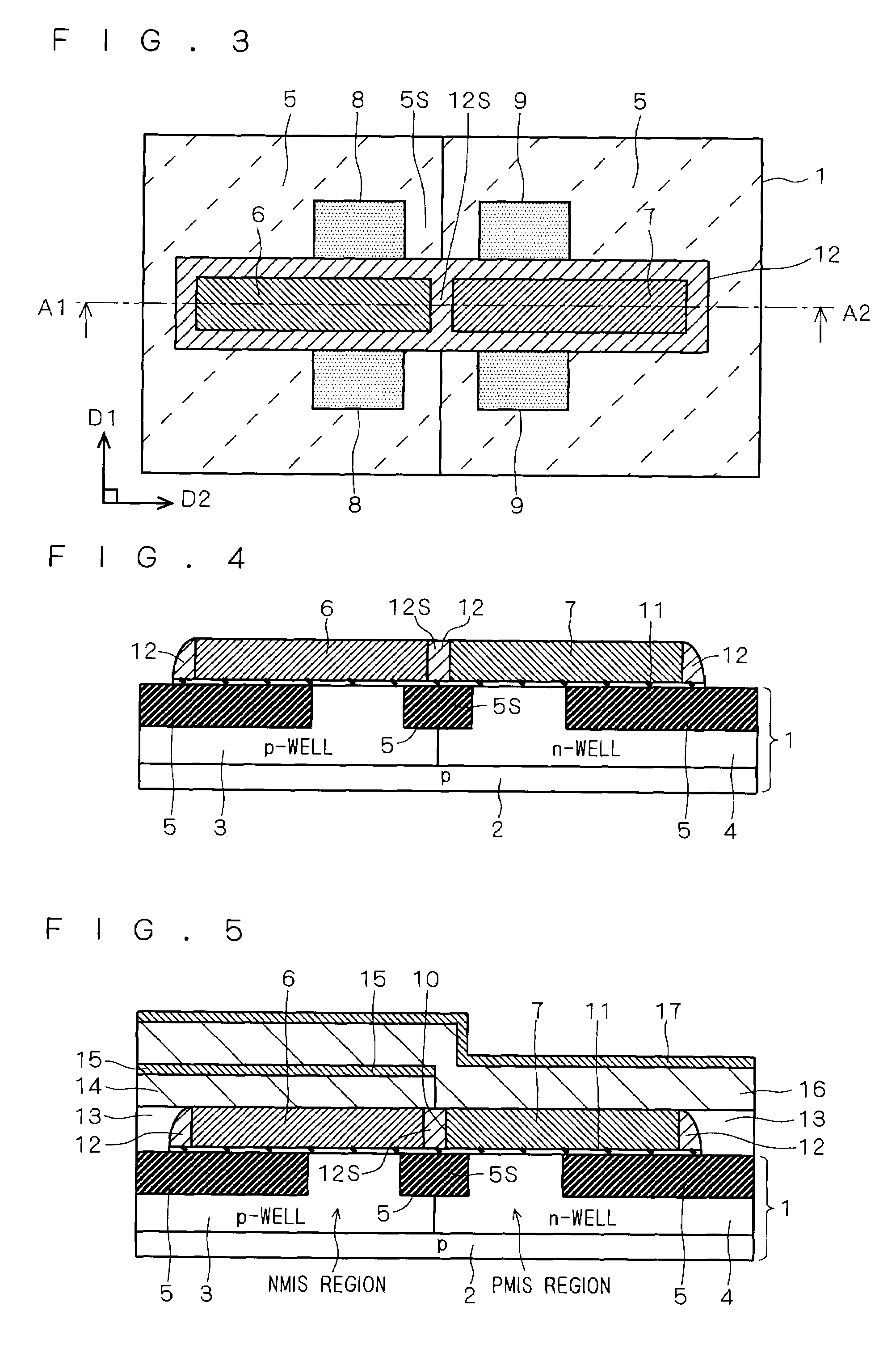
[0077]As the isolation width becomes narrower with miniaturization, setting the interval between the gate electrodes facing each other narrow in accordance with the isolation width becomes difficult in terms of limitation of lithography in the case of forming the aforementioned gap 10 (see FIG. 2) between the gate electrodes of the NMIS transistor and the PMIS transistor. The projecting amount from the active layer of the gate electrode to the isolation insulating film normally requires about 30 nm to 50 nm from the demands of lithography in order to ensure a gate length. The value combining the projection amount from both gate electrodes is 60 nm to 100 nm. As the wi...

third embodiment

Effect of Third Embodiment

[0086]According to the present embodiment, the pattern of the narrow gap 10 can be formed by facing the gate electrodes 24, 25 of both conductivity types at the PN boundary even if the width of the isolation insulating film located at the PN boundary is narrowed by miniaturization, and further miniaturization of the device can be achieved.

Fourth Embodiment

[0087]The conductive film for connecting the both gate electrodes, which is the core of the present embodiment, has a configuration of being embedded and formed in an insulating film surrounding the both gate electrodes and having the upper surface located in the same plane as the upper surfaces of the both gate electrodes, where the upper end of the conductive film and the upper ends of the both gate electrodes are substantially in plane. According to such configuration, a connection hole does not need to be formed in the inter-layer insulating film formed in the CMIS transistor, and layout restriction of...


PUM


Abstract

Gate electrodes made of polysilicon film are isolated and face each other by way of a side wall spacer portion that fills a gap formed above an isolation insulating film at the boundary of NMIS region and PMIS region. A first metal film is formed on one of the gate electrodes, and an inhomogeneous second metal film is formed on the other of the gate electrodes. The both gate electrodes become inhomogeneous metal silicide gates through the promotion of silicide reaction by heat treatment. The mutual diffusion of metal atoms from the metal film to the gate electrode is suppressed by the interposition of the side wall spacer portion being an insulating film.

Description

BACKGROUND OF THE INVENTION[0001]1. Field of the Invention[0002]The present invention relates to the field of semiconductor devices including a CMIS transistor.[0003]2. Description of the Background Art[0004]A stacked configuration of polysilicon and metal silicide has been conventionally used for the gate electrode material in response to the demand for workability and heat resistance, and easiness in threshold control of the CMIS.[0005]However, a configuration configured only from metal or metal silicide is again given attention for the gate material for higher performance of the transistor, lower resistance of the gate electrode, and suppression of gate depletion in the logic device of 45 nm or over, and is recently being actively researched and developed.[0006]In addition to lower temperature of the process in response to the demands for enhancing the performance of the transistor, and enhancement in lithography and dry etching techniques, enhancement in the new processing techn...

Claims


Application Information

Patent Timeline
Patent Type & Authority Applications(United States)
IPC IPC(8): H01L29/94H01L21/8238
CPCH01L21/28097H01L21/823842H01L21/823871H01L29/66545H01L27/11H01L27/1104H01L27/0207H10B10/00H10B10/12
Inventor TSUTSUMI, TOSHIAKIOKUDAIRA, TOMONORIKASHIHARA, KEIICHIROYAMAGUCHI, TADASHI
Owner RENESAS TECH CORP
Why Eureka
Try Eureka