Fabrication of silicon nano wires and gate-all-around MOS devices

a technology of silicon nano wires and mos, which is applied in the direction of semiconductor devices, electrical devices, nanotechnology, etc., can solve the problems of buried dielectric thickness isolating, the use of expensive soi wafers in single crystal silicon waveguides, etc., and achieves the effect of improving the surface quality

Inactive Publication Date: 2007-12-27
ECOLE POLYTECHNIQUE FEDERALE DE LAUSANNE (EPFL)
View PDF1 Cites 50 Cited by
  • Summary
  • Abstract
  • Description
  • Claims
  • Application Information

AI Technical Summary

Benefits of technology

[0011] The NWs are produced by using a hard mask of a dielectric material to etch a rib in the silicon surface. The sides of the rib are then protected by spacers consisting of one or more dielectric layers. The spacers protect the NW during the subsequent isotropic etching step. The isotropic etching step has two purposes: (i) the vertical etching defines the distance from the bottom of the NW to the s

Problems solved by technology

Therefore, the fabrication of single crystal silicon waveguides generally requires the use of expensive SOI wafers as the starting material.
However, this process requires the use of an advanced epitaxial proces

Method used


Image

  • Fabrication of silicon nano wires and gate-all-around MOS devices
  • Fabrication of silicon nano wires and gate-all-around MOS devices
  • Fabrication of silicon nano wires and gate-all-around MOS devices

Examples


Embodiment Construction

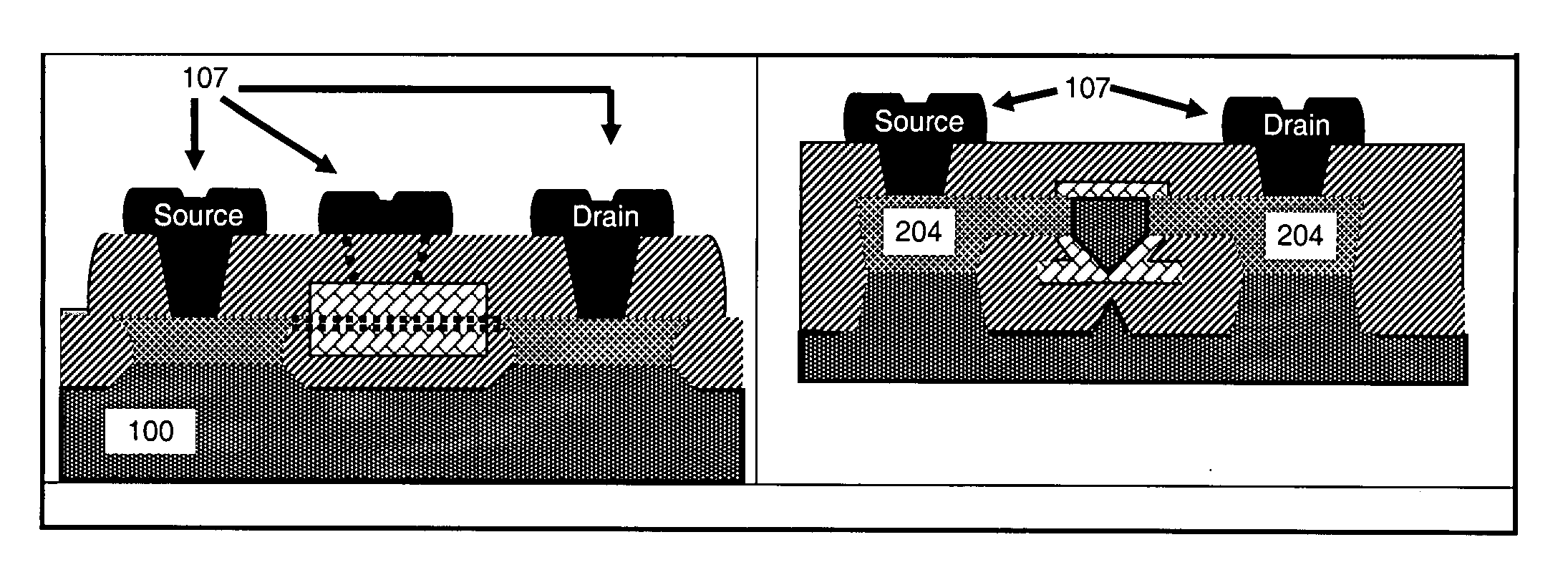
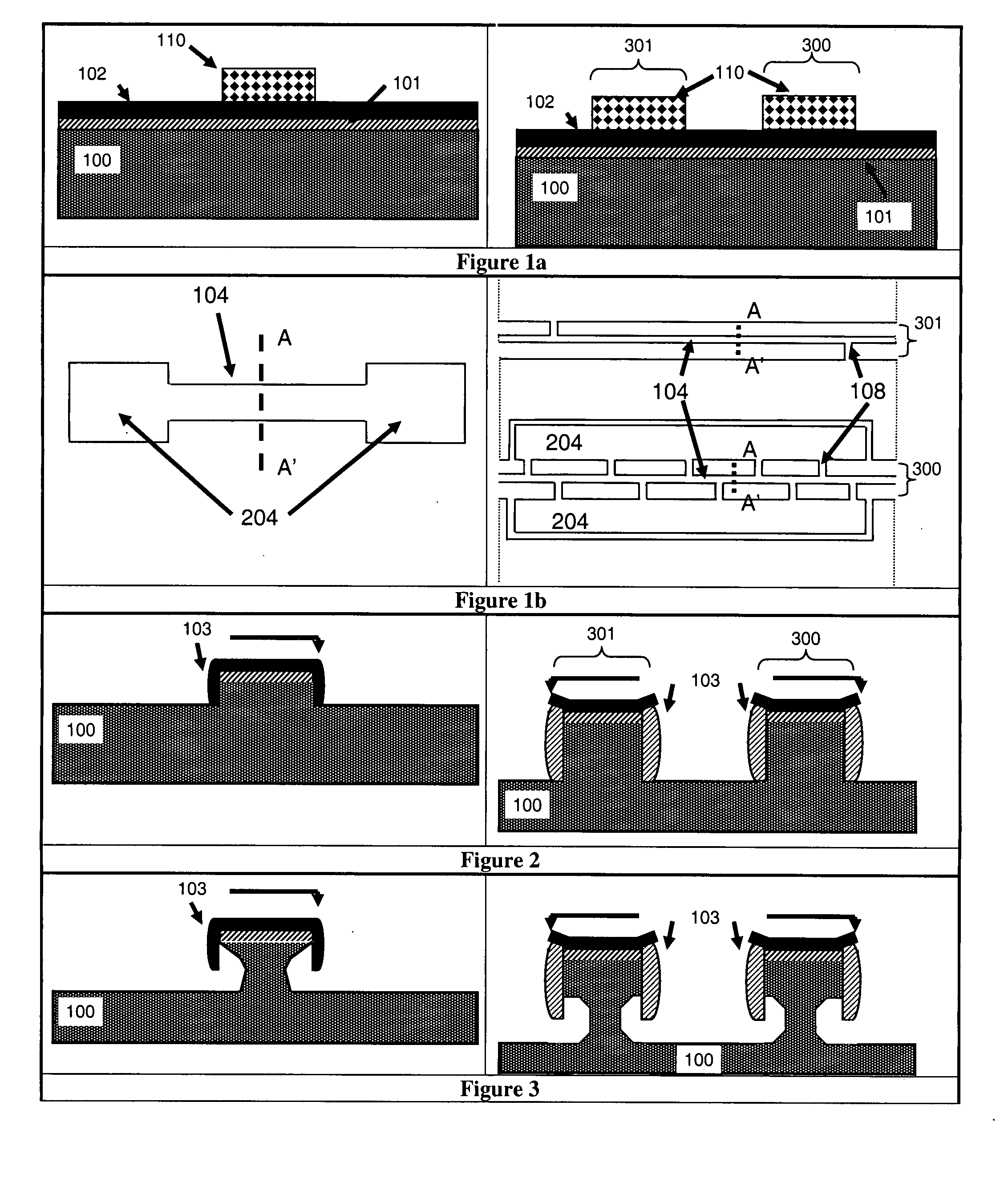
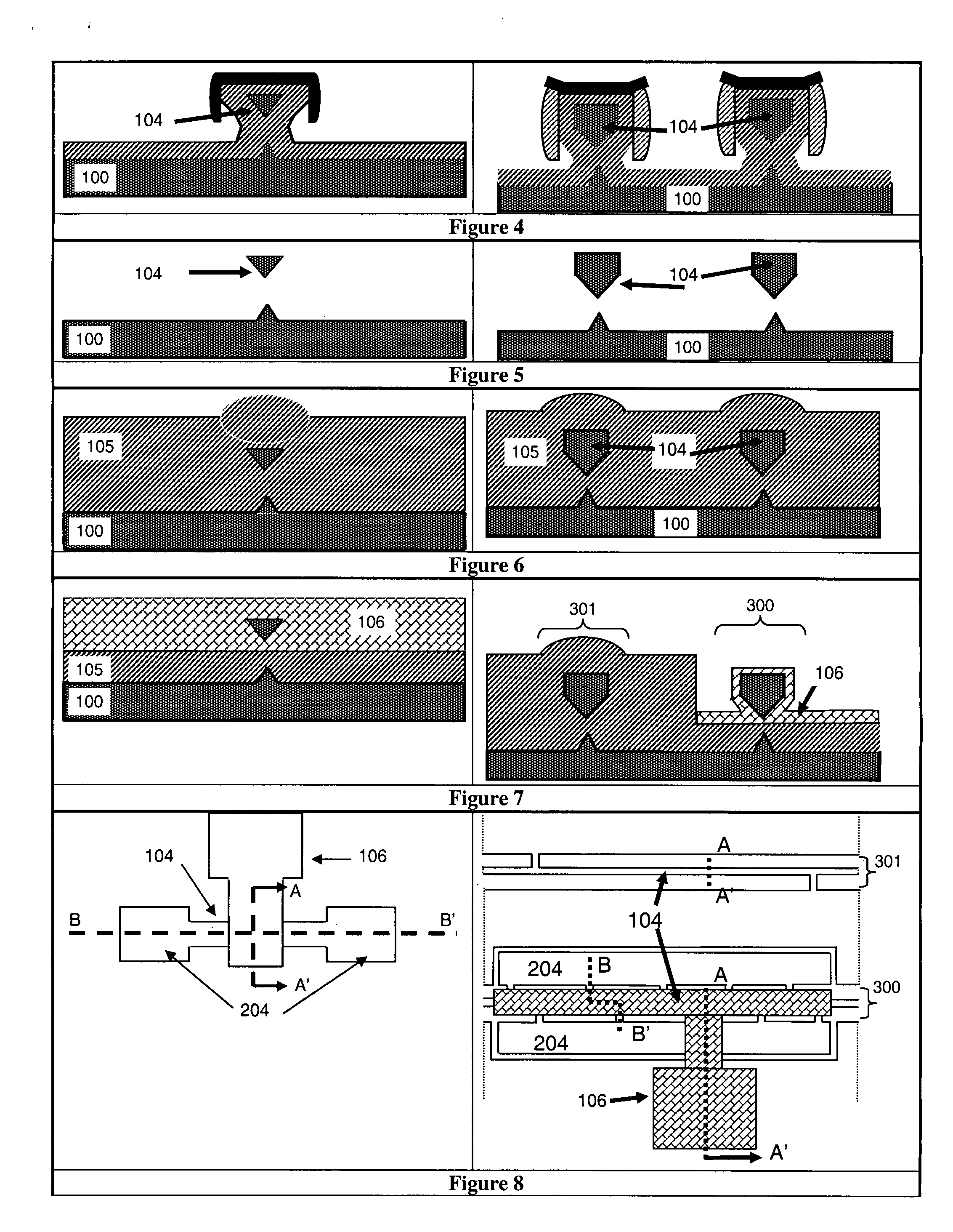
[0024] The following detailed description of the subject matter refers to the accompanying drawings. The same reference numbers may be used in different drawings to identify the same or similar elements. The drawings on the left pertain to an exemplary embodiment of the invention as a GAA MOSFET, which will be described first, whereas the drawings on the right describe an exemplary embodiment of the invention as a photonic waveguide, and an optical modulator.

[0025]FIG. 1a illustrates the cross section of a semiconductor device 100 formed in accordance with an embodiment of the present invention. Referring to FIG. 1, the semiconductor device 100 will most likely be a bulk silicon wafer, but there is nothing that hinders the use of thick SOI, SiGe or alternative technologies. A dielectric layer 101 such as silicon oxide (e.g., SiO2) may be formed over the semiconductor device 100 and then covered with a second dielectric layer 102 such as silicon nitride (Si3N4). Silicon nitride laye...


PUM

PropertyMeasurementUnit
Thicknessaaaaaaaaaa
Thicknessaaaaaaaaaa
Thicknessaaaaaaaaaa

Abstract

The invention relates to methods for manufacturing semiconductor devices. Processes are disclosed for implementing suspended single crystal silicon nano wires (NWs) using a combination of anisotropic and isotropic etches and spacer creation for sidewall protection. The core dimensions of the NWs are adjustable with the integration sequences: they can be triangular, rectangular, quasi-circular, or an alternative polygonal shape. Depending on the length of the NWs, going from the sub-micron to millimeter range, the NWs may utilize support from anchors to the side, during certain processing steps. By changing the lithographic dimensions of the anchors compared to the NWs, the anchors may be reduced or eliminated during processing. The method covers, among other things, the integration of Gate-All-Around NW (GAA-NW) MOSFETs on a bulk semiconductor. The GAA structure may consist of a silicon core fabricated as specified in the invention, surrounded by any usable gate dielectric, and finally by a gate material, such as polysilicon or metal. The source and drain of the GAA-NW may be connected to the bulk semiconductor to avoid self heating of the device over a wide range of operating conditions. The GAA-NW MOS capacitor can also be used for the integration of a Gate-All-Around optical phase modulator (GAA modulator). The working principle for the optical modulator is modulation of the refractive index by free carrier accumulation or inversion in a MOS capacitive structure, which changes the phase of the propagating light.

Description

TECHNICAL FIELD [0001] The invention relates to the fabrication of silicon nano wires and gate-all-around MOS devices, for example, using spacers and a combination of anisotropic and isotropic etching and oxidation. BACKGROUND AND SUMMARY OF THE INVENTION [0002] Nano wires (NWs) in many different materials are finding widespread applications. In some cases, they display unique physical properties not found in the bulk material (e.g., carbon nanotubes), and, in some applications, the dimensional control is used to enhance quantum effects (e.g., single electron transistors). Even for devices not exploiting the nanoscale effects, NW-based devices can offer compactness and superior performance, as compared to bulk or planar structures. [0003] Silicon NWs are used today for multiple gate transistors as well as for waveguides for optical integrated circuits on silicon-on-insulator (SOI) wafers. In the latter case, the buried insulating dielectric, with refractive index less than that of s...

Claims


Application Information

Patent Timeline
IPC IPC(8): H01L21/336C23F1/00
CPCB82Y10/00H01L29/0665H01L29/78696H01L29/42392H01L29/0673
Inventor BOUVET, DIDIERMOSELUND, KIRSTENIONESCU, MIHAI ADRIAN
Owner ECOLE POLYTECHNIQUE FEDERALE DE LAUSANNE (EPFL)
Why Eureka
Try Eureka