
Method of growing gallium nitride crystal

a gallium nitride and crystal technology, applied in the direction of single crystal growth, polycrystalline material growth, chemistry apparatus and processes, etc., can solve the problems of difficult crystal growth of gan in liquid phase, no practical size gan crystals with a diameter larger than 2 inches have been produced by liquid phase growth, and the current density of gan is large. , to achieve the effect of low defect density, low cost and low dislocation density

Inactive Publication Date: 2008-01-10
SUMITOMO ELECTRIC IND LTD
View PDF6 Cites 22 Cited by
  • Summary
  • Abstract
  • Description
  • Claims
  • Application Information

AI Technical Summary

Benefits of technology

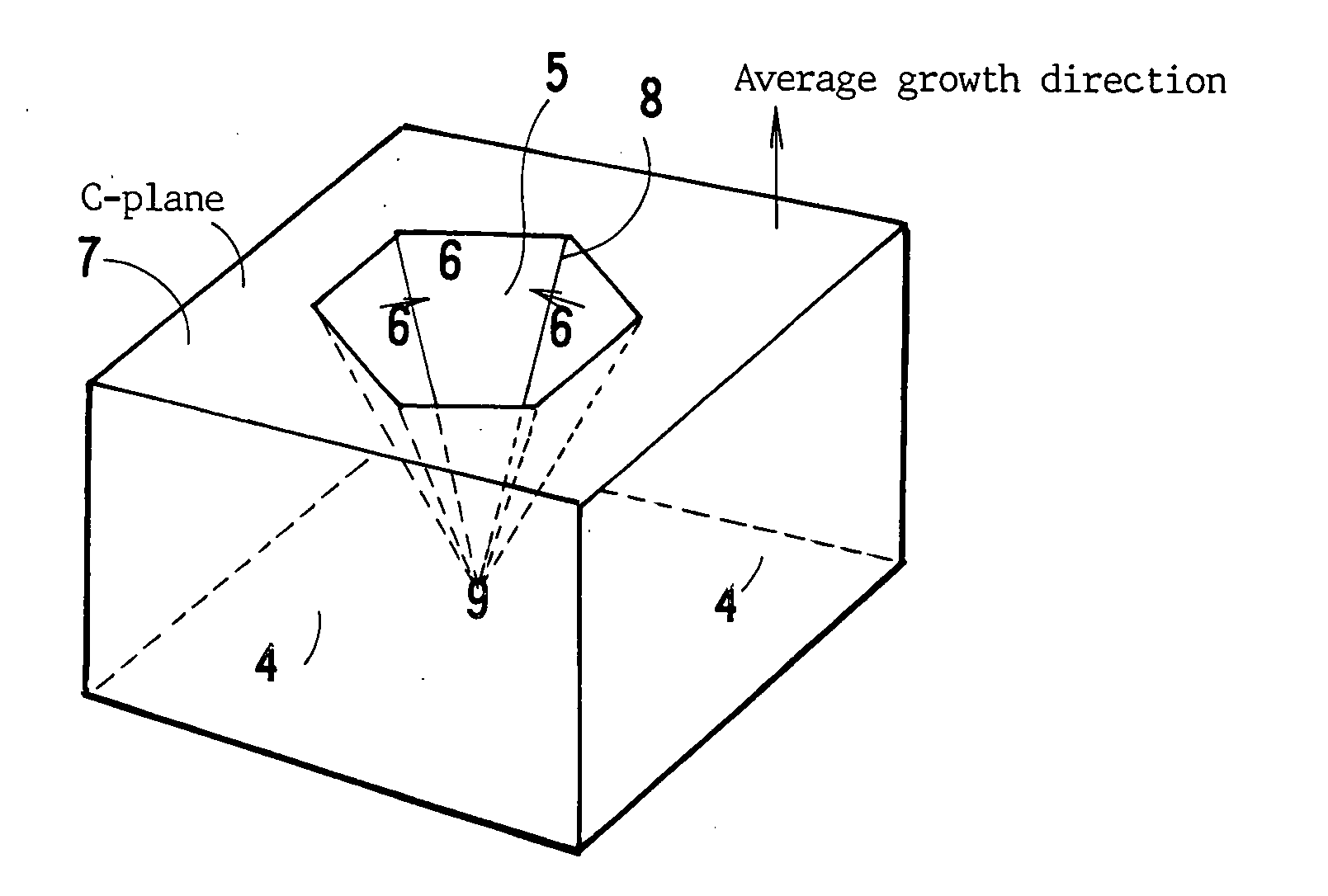
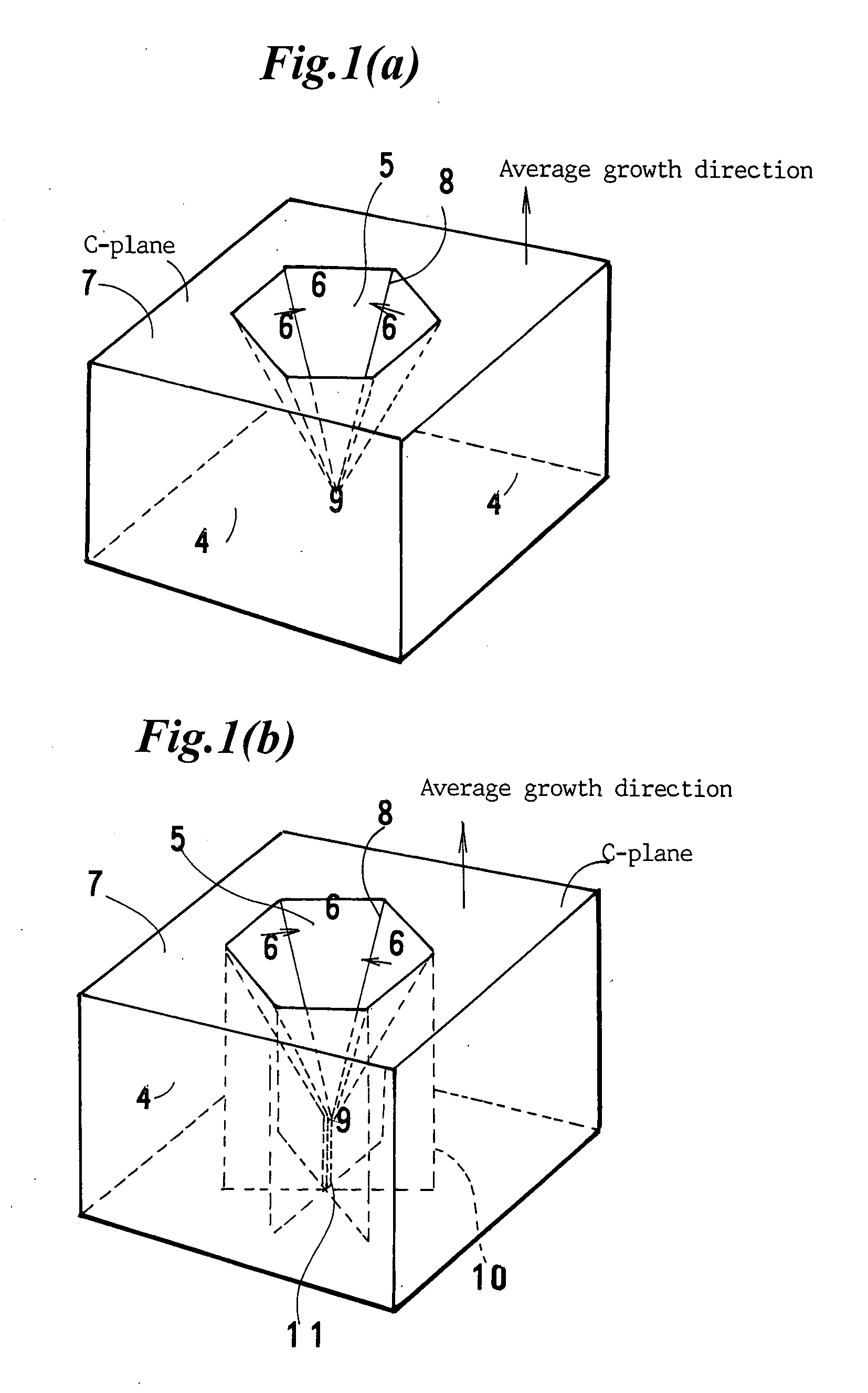
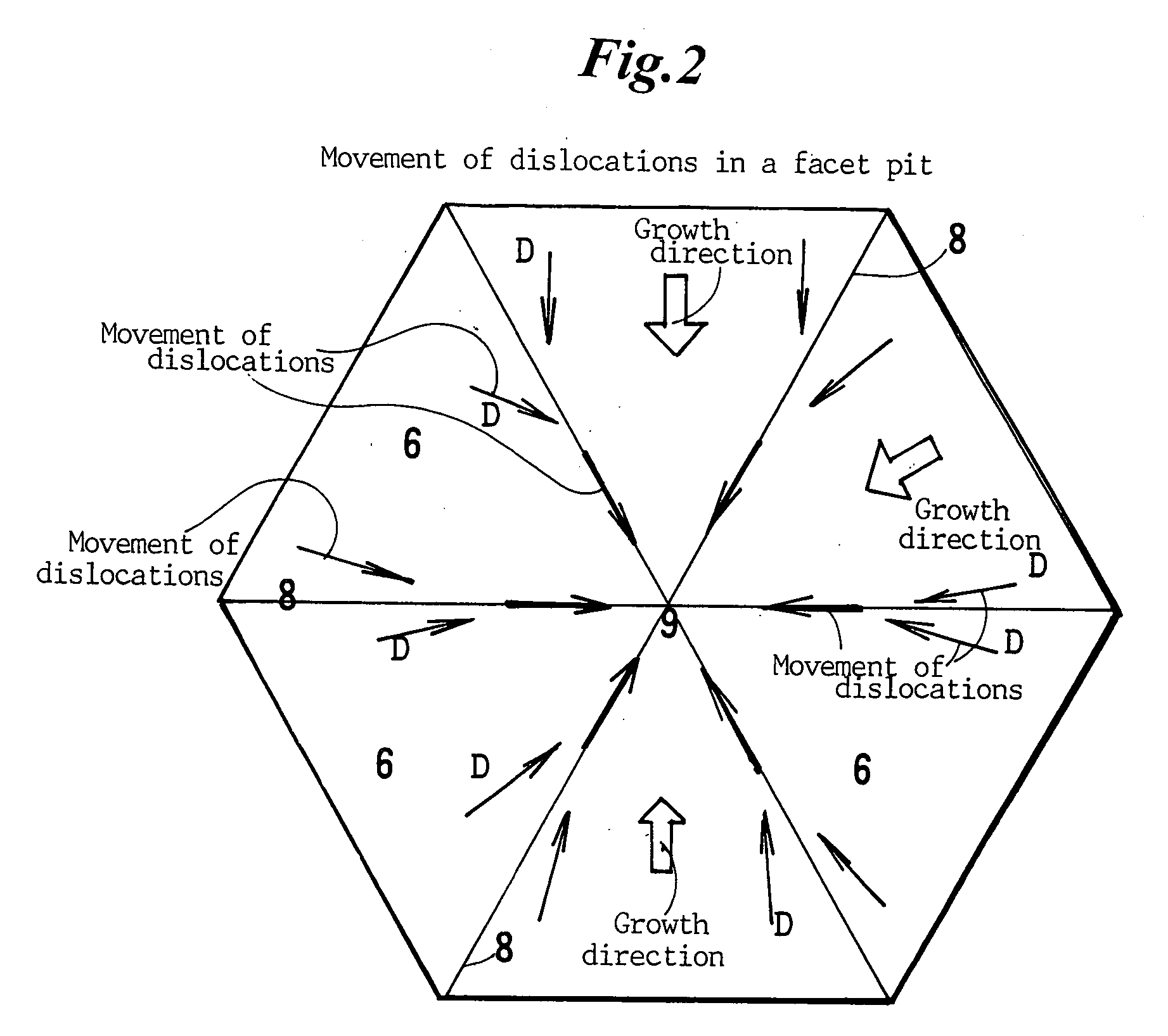
[0074] Among the four types of A, P, J and O, the present invention aims at making the inversion regions J on masks as defect accumulating regions H. The on-mask defect accumulating regions H have a function of attracting dislocations out of the neighboring GaN crystals grown below facets and arresting the dislocations in the defect accumulating regions H. The neighboring GaN crystals from which dislocations are swept become low defect density. The dislocation attracting function is the strongest in the inversion region J. Three other types of H have a weaker function of gathering / arresting dislocations than the inversion region J. The inversion region J is the best for defect accumulating regions H.
[0079] The growth which produces the inversion beaks Q and the polarity inversion regions J is called a “first growth”. The growth temperature which makes the beaks Q and the inversion regions J is called a “first growth temperature” Tj(° C.). When tiny beaks Q and inversion regions J once happen, a thick GaN crystal is grown on conventional facet growth conditions. The time required for making the inversion regions J, which depends upon the growing speed, is a short time of about 0.25 hour to 2 hours.
[0081] The inventors have discovered that a more restricted range of the first growth temperature Tj=920° C.-960° C. enbles a wide scope of different growing speeds Vj to produce inversion regions J on allover masks M. The range of Tj=920° C.-960° C. as first growing temperatures Tj is more favorable for making GaN substrate crystals in industrial scale, since the temperature range allows the facet growth to yield inversion regions J and low defect density single crystal regions Z with high stability.
[0092] High quality GaN substrates of low defect density are ardently desired. The present invention clarifies the conditions of producing inversion regions J on masks as defect accumulating regions H at an initial stage in the facet growth method composed of the steps of implanting masks M on an undersubstrate U, growing GaN in vapor phase, inducing facets on a growing GaN crystal, preparing defect accumulating regions H on the masks at pits or grooves, maintaining facet pits or facet grooves, gathering dislocations into the facet pits or the grooves and decreasing dislocation density in the surrounding regions. The present invention demonstrates requisite conditions of preparing inversion regions J on masks M. The present invention gives high quality GaN substrate crystals by adjusting the first growth temperature and the first growing speed, enabling masks to make definite inversion regions J and allowing the inversion regions J to decrease dislocations in the surrounding single crystal regions Z and Y.

Problems solved by technology

Sapphire substrates are unsuitable for GaN LDs which have large current density.
However, crystal growth of GaN in liquid phase is difficult.
No practical size GaN crystals with a diameter larger than 2 inches have been produced by liquid phase growth.
However the GaN crystals produced by the ELO methods or the HELO method of (1) have high density of dislocations and poor quality.
In these cases of polycrystal or inclining axis single crystal, the above-mask defect accumulating regions H are insufficient to work as a defect annihilating / accommodating device.
When blue / violet GaN type LDs are produced on a high defect density GaN substrate, the yield of accepted products will be low.
It is not easy to stably produce polarity inversion regions Q upon slanting facets F rising from the verges of masks.
Furthermore nobody has clarified the conditions of yielding polarity inversion crystals on growing any kinds of crystals throughout the history of crystal growth.
High dislocation density poor quality GaN crystals are made on exposed parts in the ELO.
On-mask crystals are good and off-mask crystals are poor in the ELO.
On the contrary, the facet growth makes low dislocation density good GaN crystals on exposed parts and yields high dislocation density poor GaN crystals on masks.

Method used


Image

  • Method of growing gallium nitride crystal
  • Method of growing gallium nitride crystal
  • Method of growing gallium nitride crystal

Examples


embodiment 1

Dependence of Inversion Regions J Upon First Temperature Tj

[0125] Embodiment 1 studies how the occurrence of inversion regions J depends upon the first temperature Tj, which is the temperature at the step of making inversion regions J on masks.

[1. Undersubstrates (U)]

[0126] 2 inch diameter sapphire single crystal wafers (U1), 2-inch diameter GaAs single crystal wafers (U2) and 2-inch GaN / sapphire wafers (U3) which are 1.5 μm thick GaN layer coated sapphire wafers are prepared. The sapphire wafers (U1) are C-plane ((0001) plane) surface wafers. The GaAs wafers (U2) are GaAs(111)A-plane (Ga-plane) wafers. The GaN / sapphire wafers have C-plane sapphire wafers and 1.5 μm GaN thin layers deposited thereon. GaN / sapphire wafers are sometimes called “templates”.

[2. Mask Patterns (M)]

[0127] Masks should have a property of inhibiting GaN from epitaxial growing. 0.1 μm thick SiO2 layers are deposited on three kinds of undersubstrates U1, U2 and U3. Photolithography and etching pattern the ...

embodiment 2

Dependence on Growing Speeds Vj at a Temperature of 940

[0174] Embodiment 2 uses the same HVPE growth furnace as Embodiment 1. Embodiment 2 employs stripe / dotmasked GaAs(111) undersubstrates M1U2 and M2U2 prepared by forming an SiO2 stripemask M1 or SiO2 dotmask M2 on GaAs(111) undersubstrates U2. Embodiment 2 grows GaN crystals on the stripemasked and dotmasked undersubstrates by varying the growing speed Vj at a temperature of 940. Embodiment 2 investigates relations between the growing speed Vj and the facility of forming the orientation inversion regions J at 940.

[0175] The stripe / dotmasked undersubstrates M1U2 and M2U2 are laid on a susceptor in the HVPE reaction furnace. At an initial step, GaN buffer layers are grown on the undersubstrates for 15 minutes at a low temperature Tb of about Tb=500 by supplying HCl and NH3 at a NH3 partial pressure PNH3=0.2 atm (20 kPa) and an HCl partial pressure PHCl=2×10⁻³ atm (0.2 kPa). The thicknesses of the buffer layers are about 60 nm.

[0...

embodiment 3

Dependence on Growing Speeds at a Temperature of 1030

[0204] Repetitions of trials of Embodiments 1 and 2 suggest the inventors that the facility of inducing inversion regions J depends strongly upon the temperature Tj firstly and depends upon the growing speeds Vj at the temperature Tj secondarily. Embodiment 3 investigates dependence of inversion region occurrence upon growing speeds at a temperature of 1030 higher than Embodiment 2 (940).

[0205] Embodiment 3 uses the same HVPE growth furnace as Embodiment 1. Embodiment 3 employs stripe / dotmasked GaAs(111) undersubstrates M1U2 and M2U2 prepared by forming an SiO2 stripemask M1 or an SiO2 dotmask M2 on GaAs(111) undersubstrates U2. Embodiment 3 grows GaN crystals on the stripemasked and dotmasked undersubstrates by varying the growing speed at a temperature of 1030 different from Embodiment 2 (940). Embodiment 3 investigates relations between the growing speed and the facility of forming the orientation inversion regions J at 1030....


PUM


Abstract

The facet growth method grows GaN crystals by preparing an undersubstrate, forming a dotmask or a stripemask on the undersubstrate, growing GaN in vapor phase, causing GaN growth on exposed parts, suppressing GaN from growing on masks, inducing facets starting from edges of the masks and rising to tops of GaN crystals on exposed parts, maintaining the facets, making defect accumulating regions H on masked parts. attracting dislocations into the defect accumulating regions H on masks and reducing dislocation density of the surrounding GaN crystals on exposed parts. The defect accumulating regions H on masks have four types. The best of the defect accumulating regions H is an inversion region J. Occurrence of the inversion regions J requires preceding appearance of beaks with inversion orientation on the facets. Sufficient inversion regions J are produced at an initial stage by maintaining the temperature Tj at 900° C. to 990° C. without fail. Allowable inversion regions J beaks are produced at an initial stage by the sets of temperatures T(K) and growing speeds Vj (μm / h) satisfying −4.39×10⁵ / T+3.87×10²<Vj<−7.36×10⁵ / T+7.37×10².

Description

RELATED APPLICATIONS [0001] This application is a Continuation-In-Part Application based on U.S. patent application Ser. No. 10 / 933,291 filed Sep. 3, 2004 and U.S. patent application Ser. No. 10 / 936,512 filed Sep. 9, 2004.[0002] This application claims priority to Japanese Patent Application No. 2006-210506 filed Aug. 2, 2006. FIELD OF THE INVENTION [0003] Gallium nitride (GaN) type blue / violet semiconductor lasers will be used for reading-out data of the next generation large capacity photodiscs. Putting GaN type blue / violet laser diodes (LDs) into practice requires gallium nitride crystal substrates of high quality. This invention relates to a method of growing a high quality gallium nitride crystal (GaN) for substrate wafers on which blue / violet LDs are made. In addition to production of GaN blue / violet LDs, the GaN substrate wafers will be useful for producing light emitting devices (light emitting diodes LEDs, laser diodes LDs of other colors), electronics devices (rectifiers, ...

Claims


Application Information

Patent Timeline
IPC IPC(8): C30B25/04
CPCC30B25/183C30B23/025
Inventor HIROTA, RYUMOTOKI, KENSAKUNAKAHATA, SEIJIOKAHISA, TAKUJIUEMATSU, KOJI
Owner SUMITOMO ELECTRIC IND LTD
Learn More