Wiring board and semiconductor device excellent in folding endurance

a semiconductor device and wire technology, applied in the incorporation of printed electric components, non-metallic protective coating applications, chemistry apparatus and processes, etc., can solve the problems of high price, inability to cope with price reduction of electronic products such as liquid crystal display apparatuses, and high price of rolled copper foils. achieve excellent folding endurance and high fineness

Inactive Publication Date: 2008-01-10
MITSUI MINING & SMELTING CO LTD
View PDF29 Cites 8 Cited by
  • Summary
  • Abstract
  • Description
  • Claims
  • Application Information

AI Technical Summary

Benefits of technology

[0012] An object of the present invention is to provide a wiring board and a semiconductor device in which

Problems solved by technology

Rolled copper foils as described above, however, are high in price as compared with electrodeposited copper foils, so the use of rolled copper foils cannot cope with price lowering of electronic products such as liquid crystal display apparatuses.
Consequently, wire breakage tends to take place in the folded portion, near the ACF edge and in the vicinity of the connection terminals.
In particular, wire breakage is more frequent when the wiring pattern has inner leads at pitches of less than 35 μm, because formation of such fine wiring pattern entails

Method used


Image

  • Wiring board and semiconductor device excellent in folding endurance
  • Wiring board and semiconductor device excellent in folding endurance

Examples


example 1

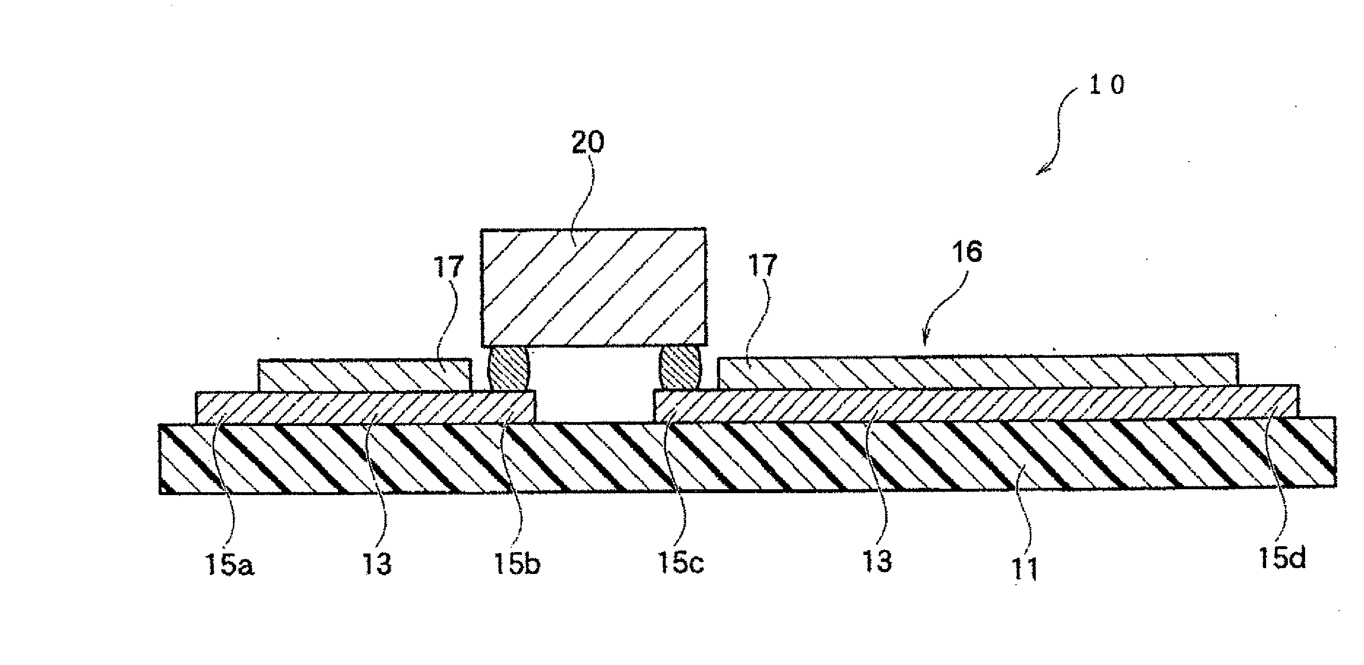
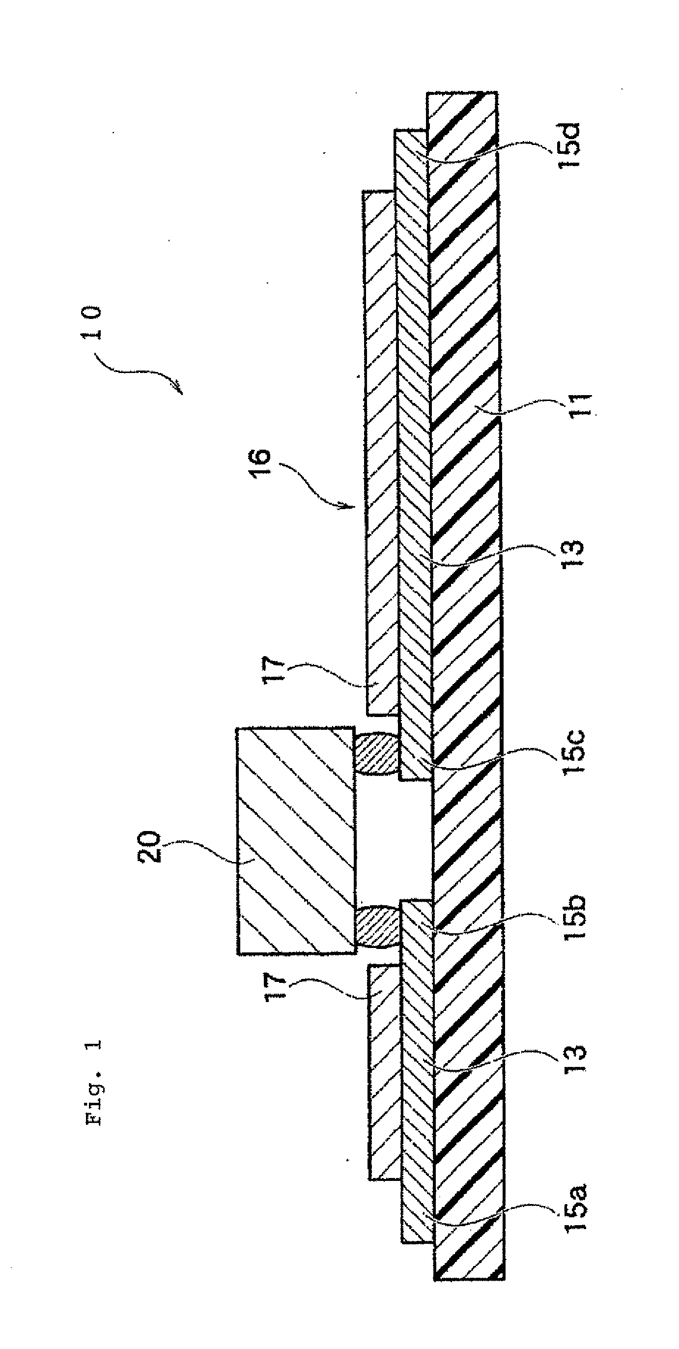
[0072] First, copper was deposited at a thickness of 12 μm on a drum-like electrode at a solution temperature of 50° C. at a current density of 60 A / dm2 by means of a sulfuric acid-based copper electrolytic solution having a copper concentration of 80 g / liter, a free sulfuric acid concentration of 140 g / liter, a 1,3-mercapto-1-propanesulfonic acid concentration of 4 ppm, a diallyldimethylammonium chloride (Available from Senka Corp., Unisense FPA100L) concentration of 3 ppm and a chloride concentration of 10 ppm, thereby producing an electrodeposited copper foil. The M face of this electrodeposited copper foil was roughened by nodule plating treatment and coverplating treatment to adjust the surface roughness (Rz) of the M face to 1.5 μm.

[0073] A polyimide resin precursor was applied on the M face of this electrodeposited copper foil and the coating was heated at 350° C. for 60 minutes to give a polyimide film 38 μm in thickness. Consequently, a board film was produced which was a ...

examples 2 and 3

[0084] A seed metal layer comprised of Cr and Ni was sputtered on a polyimide film having a tensile strength of 520 MPa, a Young's modulus of 9300 MPa and a thickness of 34.2 μm (Example 2) or 34.0 μm (Example 3). Copper was deposited on the surface of this seed metal layer by plating to produce a metal layer (Ni—Cr, Cu) at a thickness shown in Table 1, thereby producing a substrate film. A wiring board was produced as in Example 1 except that this substrate film was used. The polyimide film used herein comprised a polyimide obtained by use of biphenyltetracarboxylic dianhydride as a tetracarboxylic dianhydride component.

[0085] The wiring board was tested with use of an MIT testing apparatus in the same manner as in Example 1. The results are shown in Table 2.

example 5

[0092] A seed metal layer comprised of Cr and Ni was sputtered on a polyimide film having a tensile strength of 520 MPa, a Young's modulus of 9300 MPa and a thickness of 34.2 μm. Copper was deposited on the surface of this seed metal layer by plating to produce a metal layer (Ni—Cr, Cu) at a thickness of 7.6 μm as shown in Table 3, thereby producing a board film. A wiring pattern was produced as in Example 1 except that this substrate film was used. The polyimide film used herein comprised a polyimide obtained by use of biphenyltetracarboxylic dianhydride as a tetracarboxylic dianhydride component.

[0093] The thickness of the wiring pattern was 7.6 μm, and a solder resist layer was formed at a thickness of 37.5 μm. The thickness of the solder resist layer (37.5 μm) was 110% relative to the thickness of the polyimide film (34.2 μm).

[0094] The wiring board was tested with use of an MIT testing apparatus in the same manner as in Example 1. The results are shown in Table 4.


PUM

PropertyMeasurementUnit
Lengthaaaaaaaaaa
Lengthaaaaaaaaaa
Lengthaaaaaaaaaa

Abstract

A wiring board with folding endurance includes an insulating film and a copper-containing wiring pattern on a surface of the insulating film, and includes an insulating resin coating layer formed on the wiring pattern such that terminals are exposed. The wiring board has any of the constitutions (A), (B), (C) and (D) below. (A) The wiring pattern includes copper particles having a mean crystal particle diameter in the range of from 0.65 to 0.85 μm as determined by EBSP; not more than 1% of the volume of the wiring pattern is accounted for by copper crystal particles having a particle diameter of less than 1.0 μm as determined by EBSP; and copper crystal particles that are [100] oriented in the longitudinal direction of a lead of the wiring pattern account for from 10 to 20% of the volume of the wiring pattern as determined by EBSP. (B) The insulating film is formed of a polyimide film having a tensile strength within the range of from 450 to 600 MPa and a Young's modulus within the range of from 8500 to 9500 MPa. (C) The insulating film is formed of a polyimide film having a thickness of from 10 to 30 μm. (D) The insulating resin coating layer has a thickness of from 50 to 150% relative to the thickness of the insulating film.

Description

BACKGROUND OF THE INVENTION [0001] 1. Field of the Invention [0002] The present invention relates to a wiring board and a semiconductor device excellent in folding endurance. More specifically, the present invention relates to a wiring board and a semiconductor device having the wiring board and a semiconductor chip mounted thereon, in which breakage of wire is prevented even if the semiconductor device is folded when installed into electronic equipment or even if the semiconductor device is subjected to repeated stress by vibration, etc. during use of the electronic equipment. [0003] 2. Description of the Related Art [0004] Semiconductor chips are used for driving display apparatuses such as liquid crystal display apparatuses and PDP (Plasma Display Monitor Panel). Such a semiconductor chip is mounted on a wiring board produced by forming a wiring pattern on the surface of an insulating film and is installed in an electronic apparatus. It is necessary that the semiconductor chips a...

Claims


Application Information

Patent Timeline
IPC IPC(8): H05K1/16
CPCH01L2224/16H01L2924/01078H01L2924/09701H05K1/032H05K1/09H01L2924/01019H05K2201/0154H05K2201/0191H05K2201/0355H05K2201/10674H05K3/28H01L2924/00011H01L2924/00014H01L2224/0401B32B15/08H05K3/00
Inventor YAMAGATA, MAKOTOKURIHARA, HIROAKIYASUI, NAOYAIWATA, NORIAKI
Owner MITSUI MINING & SMELTING CO LTD
Why Eureka
Try Eureka