
Moisture barrier coatings for organic light emitting diode devices

a technology of organic light-emitting diodes and barrier films, which is applied in the field of barrier films, can solve the problems of metals typically lacking transparency, glass lacking flexibility, and oled devices suffering reduced output or premature failur

Inactive Publication Date: 2008-01-10
3M INNOVATIVE PROPERTIES CO
View PDF85 Cites 79 Cited by
  • Summary
  • Abstract
  • Description
  • Claims
  • Application Information

AI Technical Summary

Problems solved by technology

Organic light emitting diode (OLED) devices can suffer reduced output or premature failure when exposed to water vapor or oxygen.
Metals and glasses have been used to encapsulate and prolong the life of OLED devices, but metals typically lack transparency and glass lacks flexibility.
Barrier performance of the coatings deposited by these methods typically results in a moisture vapor transmission rate (MVTR) in the range from 0.1-5 g / m2 day, depending on the specific processes.

Method used


Image

  • Moisture barrier coatings for organic light emitting diode devices
  • Moisture barrier coatings for organic light emitting diode devices
  • Moisture barrier coatings for organic light emitting diode devices

Examples


example 1

[0070]Table 1 provides a description of abbreviations used in the present specification.

TABLE 1AbbreviationDescription / Commercial SourceNPDN,N′-bis(3-naphthalen-2-yl)-N,N′-bis(phenyl)benzidineavailable from H.W. Sands Corp, Jupiter, FLAlQTris(8-hydroxyquinoline) aluminum availablefrom H.W. Sands Corp, Jupiter, FLC545TCoumarin available from Eastman Kodak Co., Rochester,NY as Coumarin 545TFTCNQTetrafluoro-tetracyanoquinodimethane available fromTokyo Kasei Kogyo Co., Tokyo, JapanLiFLithium fluoride, 99.85%, available from Alfa Aesar,Ward Hill, MAAlPuratronic aluminum shots, 99.999%, available from AlfaAesar, Ward Hill, MAMTDATA4,4′,4″-tris(N-3-methylphenyl-N-phenylamino)triphenylamine, sublimed, availablefrom H.W. Sands Corp., Jupiter, FLAgPremion silver shot, 99.999% available from Alfa Aesar,Ward Hill, MACrPuratronic chromium pieces, 99.997% available fromAlfa Aesar, Ward Hill, MATMSTetramethylsilane, NMR grade, 99.9% available fromSigma-Aldrich, Milwaukee, WISiOSilicon monoxide, 99...

example 2

[0078]Top emitting OLEDs containing four independently addressable 5 mm×5 mm pixels were fabricated on ultrabarrier substrates by conventional thermal vapor deposition through shadow masks in a bell jar evaporator evacuated to 5×10⁻⁶ torr. Reflective anodes were first created by depositing Cr (100 Å at 1 Å / s) followed by Ag (1000 Å at 1 Å / s). The OLED device layers deposited on top of the Cr / Ag anodes were (in order of deposition): MTDATA doped with FTCNQ (2.8% doping, 3000 Å at 1.8 Å / s) / NPD (400 Å at 1 Å / s) / AlQ doped with C545T (1% doping, 300 Å at 1 Å / s) / AlQ (200 Å at 1 Å / s) / LiF(7Å at 0.5 Å / s) / Al(50 Å at 5 Å / s) / Ag(200 Å at 1 Å / s).

[0079]An four pixel top emitting green OLED on an ultrabarrier substrate film, such as those described above, was encapsulated by laminating a second ultrabarrier film over the pixel area using pressure-sensitive adhesive (PSA) transfer adhesive film (3M 8141 Optical Adhesive). The ultrabarrier layers faced the OLED device structure. The device was placed...

example 3

[0080]A square (approximately 35 mm) piece of ultrabarrier film was laminated to the center of a larger square (approximately 50 mm) of ultrabarrier film using a square (approximately 35 mm) gasket of PSA transfer adhesive film (3M 8141 Optical Adhesive). The ultrabarrier layers faced each other. The width of the gasket was approximately 5 mm which left a square (approximately 25 mm) cavity between the two ultrabarrier films. The construction was placed in the DLF chamber in the same manner as described in Example 1 with the surface bearing the smaller ultrabarrier film facing upwards. The system was pumped to base pressure (below about 1×10⁻³ Torr) and oxygen gas was introduced at a flow rate of 250 sccm. The sample surface was primed by a 10 second exposure to an oxygen plasma (200 watt RF power). Tetramethylsilane gas was then introduced (50 sccm) while maintaining the oxygen flow at 250 sccm. A plasma was struck at 200 watts for 5 minutes to provide a diamond-like film on the fi...


PUM


Abstract

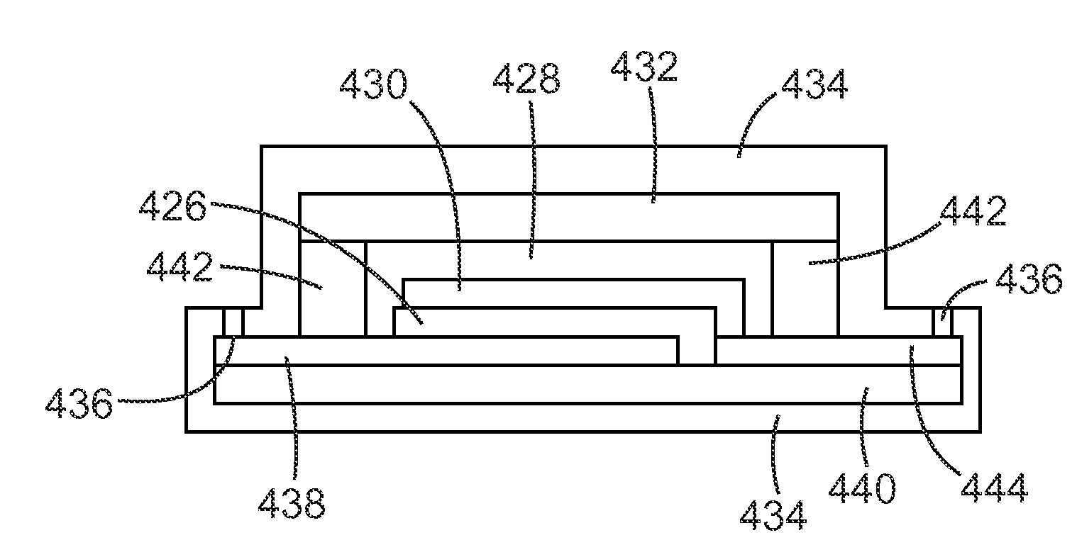
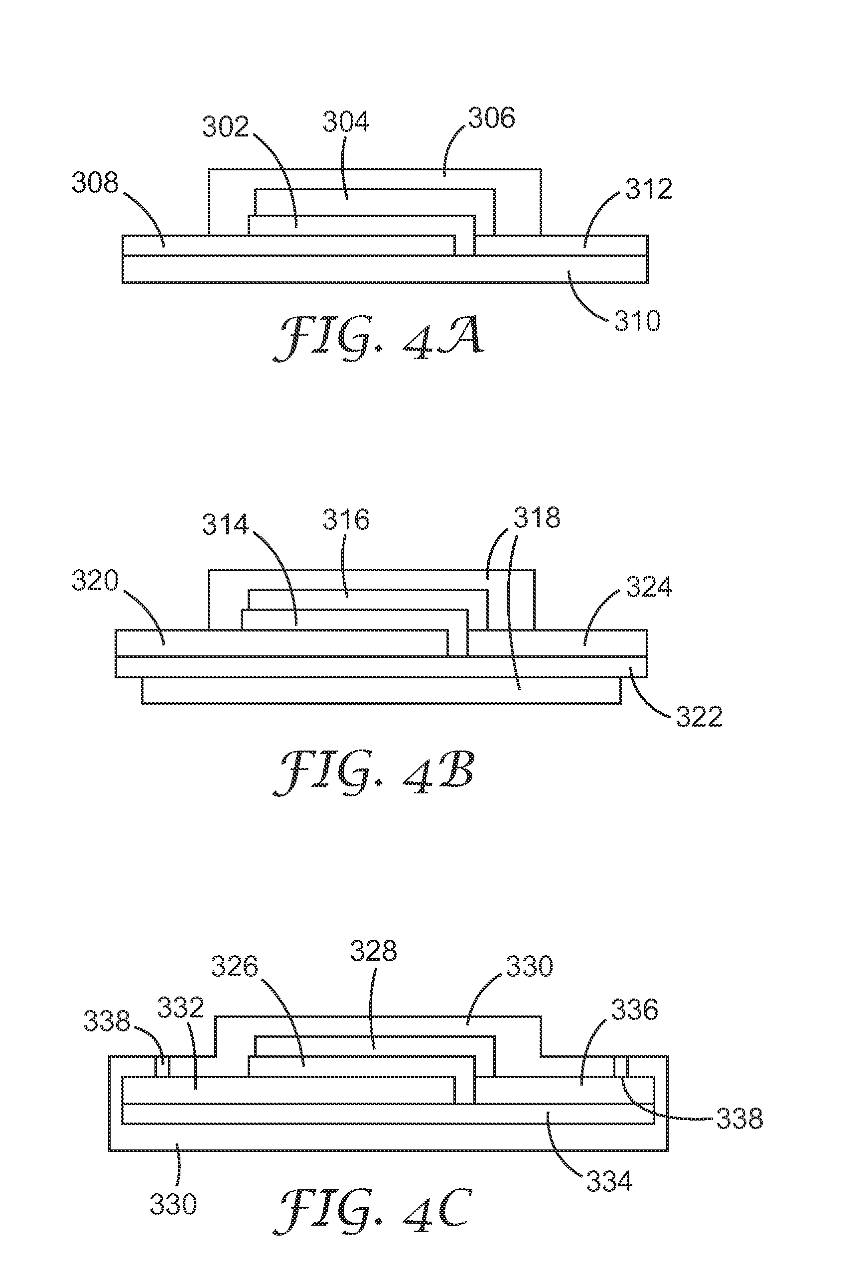
A barrier assembly having a flexible or rigid substrate, an organic electronic device, and one or more layers of diamond-like film. The diamond-like film layers can be used to mount, cover, encapsulate or form composite assemblies for protection of moisture or oxygen sensitive articles such as organic light emitting diode devices, photovoltaic devices, organic transistors, and inorganic thin film transistors. The diamond-like film layers can also provide for edge sealing of adhesive bond lines in the assemblies.

Description

FIELD OF INVENTION[0001]The present invention relates to barrier films for protection of moisture or oxygen sensitive articles such as OLED devices.BACKGROUND[0002]Organic light emitting diode (OLED) devices can suffer reduced output or premature failure when exposed to water vapor or oxygen. Metals and glasses have been used to encapsulate and prolong the life of OLED devices, but metals typically lack transparency and glass lacks flexibility. Intense efforts are underway to find alternative encapsulation materials for OLEDs and other electronic devices. Examples of various types of vacuum processes are described in the patent and technical literature for the formation of barrier coatings. These methods span the range of e-beam evaporation, thermal evaporation, electron-cyclotron resonance plasma-enhanced chemical vapor deposition (PECVD), magnetically enhanced PECVD, reactive sputtering, and others. Barrier performance of the coatings deposited by these methods typically results i...

Claims


Application Information

Patent Timeline
Patent Type & Authority Applications(United States)
IPC IPC(8): H01L29/08H01L35/24H01L51/00H10N10/856
CPCH01L51/5237H10K50/8445H05B33/04H10K50/84
Inventor MCCORMICK, FRED B.DAVID, MOSES M.ROEHRIG, MARK A.NIRMAL, MANOJ
Owner 3M INNOVATIVE PROPERTIES CO
Learn More