Method and an Apparatus for Manufacturing an Electronic Thin-Film Component and an Electronic Thin-Film Component

a technology of electronic thin film and manufacturing method, which is applied in the direction of sustainable manufacturing/processing, final product manufacturing, conductive pattern formation, etc., can solve the problems of complex mounting of electric components on circuit boards, increased difficulty in positioning components and soldering techniques for electrical contacts, and atypical deviation of materials used in these solutions, etc., to facilitate contact cutting, narrow line width, and efficient utilization of substrate surface area

Inactive Publication Date: 2008-01-17
AVANTONE OY
View PDF3 Cites 40 Cited by
  • Summary
  • Abstract
  • Description
  • Claims
  • Application Information

AI Technical Summary

Benefits of technology

[0027]As to the pressing plate arranged around the pressing block functioning as a machining member, or in roll-to-roll processes around a reel or the like, an advantageous structure is such in which “side walls” substantially vertical to the plane of the surface are used in the relief to attain the necessary variations in height, and to form sharp edges that cut well the conductive layer. This vertical character of the side walls significantly facilitates the cutting of the contact between the different conductive a...

Problems solved by technology

This, in turn, complicates the mounting of electric components on circuit boards, because the positioning of the components and the soldering technique required for the electrical contacts become more challenging.
The materials used in these solutions also typically deviate to some extent from silicon-ba...

Method used


Image

  • Method and an Apparatus for Manufacturing an Electronic Thin-Film Component and an Electronic Thin-Film Component
  • Method and an Apparatus for Manufacturing an Electronic Thin-Film Component and an Electronic Thin-Film Component
  • Method and an Apparatus for Manufacturing an Electronic Thin-Film Component and an Electronic Thin-Film Component

Examples


Embodiment Construction

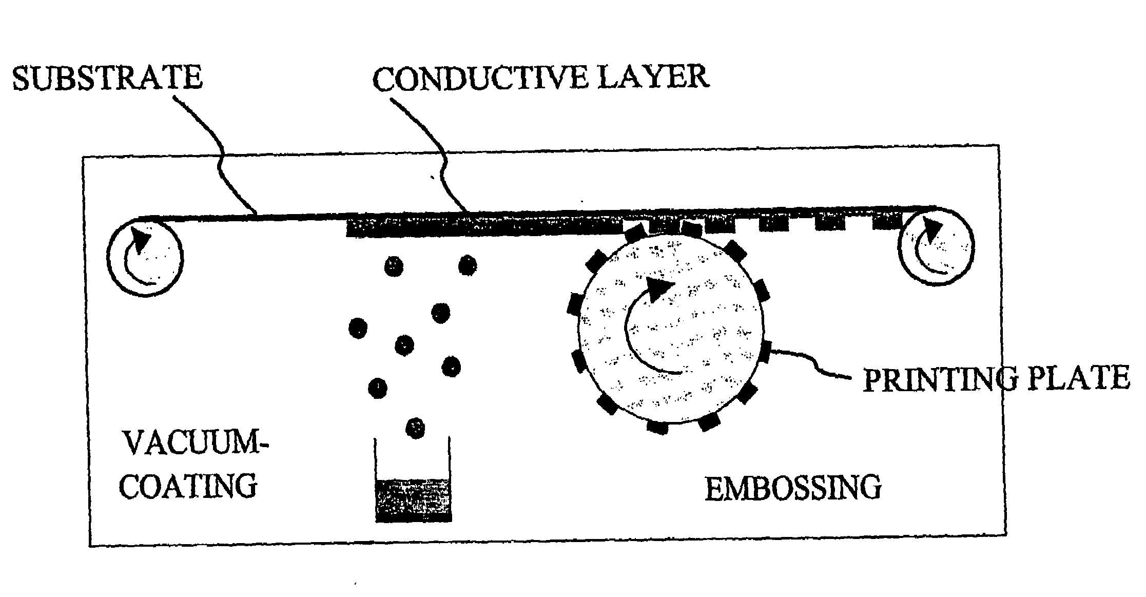
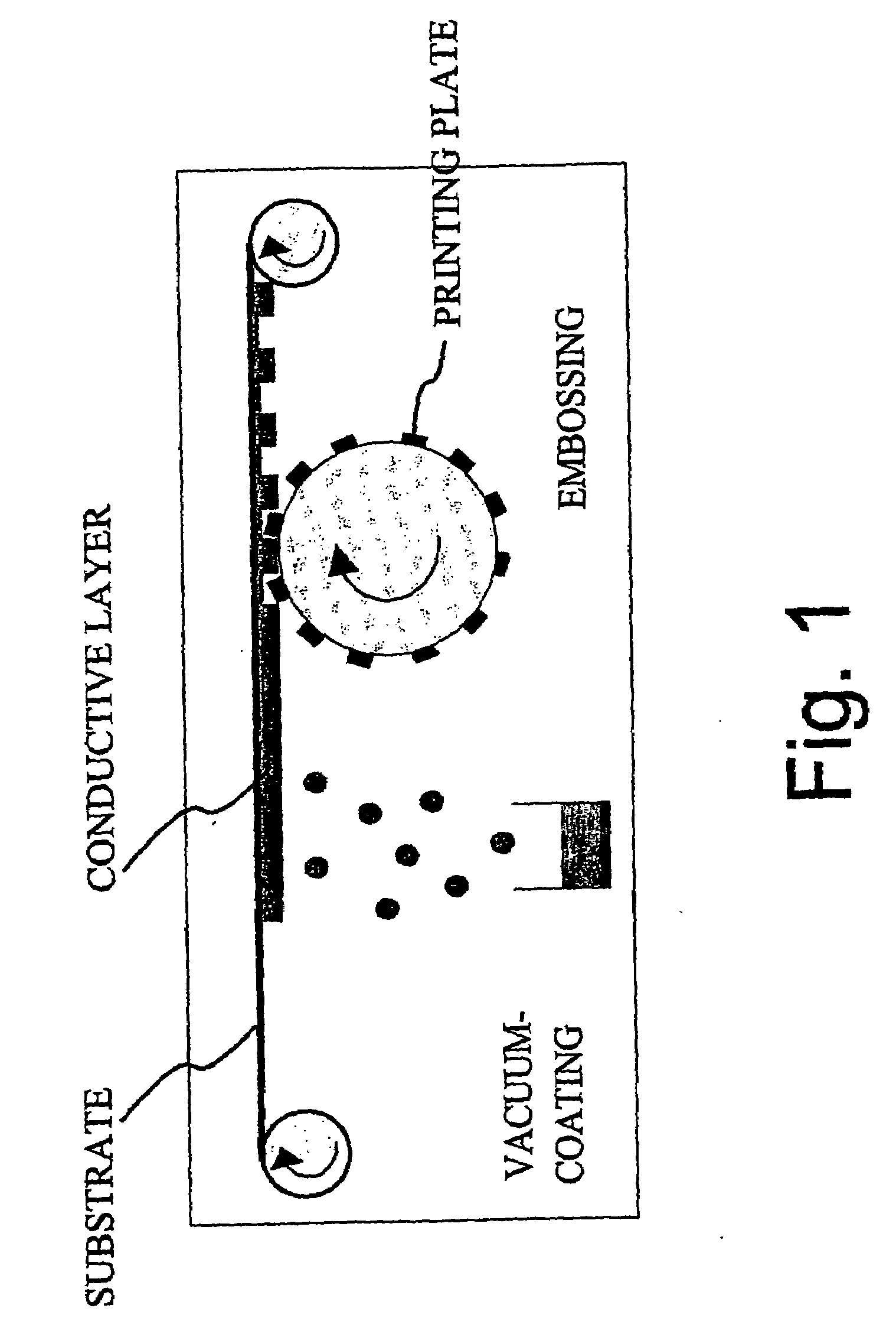
[0042]FIG. 1 shows, in principle, a roll-to-roll process, in which a plastic functioning as a substrate is first vacuum coated with a conductive layer, and thereafter an electrode pattern is formed in said conductive layer by embossing in connection with the same vacuum process by means of a pressing plate arranged around a reel or the like. The tests conducted by the applicant have shown that by means of embossing it is possible to manufacture very narrow line structures in the order of 1 to 50 μm in width on a vacuum coated plastic substrate.

[0043]FIG. 1 shows, in principle, that both the vacuum coating and the embossing are arranged to take place in the same chamber. This is not, however, the only possible embodiment of the invention, but in view of mass production the central aspect is primarily that it is possible to convey the substrate from one roll to another in one single run without having to move the rolls / substrate into different processing devices every now and then. Th...


PUM

PropertyMeasurementUnit
Widthaaaaaaaaaa
Depthaaaaaaaaaa
Distanceaaaaaaaaaa

Abstract

A method for manufacturing an electronic thin-film component, an apparatus implementing the method, and an electronic thin-film component manufactured according to the method. A lowermost, galvanically uniform conductive layer of electrically conductive material is first formed on a substantially dielectric substrate, from which lowermost conductive layer conductive areas are galvanically separated from each other to form an electrode pattern. On top of the electrode pattern it is then possible to form one or several upper passive or active layers required in the thin-film component. The separation of the lowermost conductive layer into an electrode pattern takes place by exerting on the lowermost conductive layer a machining operation based on die-cut embossing, i.e. embossing, wherein the relief of the machining member used in the machining operation causes a permanent deformation on the substrate and at the same time embosses areas from the conductive layer into conductive areas galvanically separated from each other. The method and apparatus are suitable for manufacturing thin-film components in a roll-to-roll process.

Description

FIELD OF THE INVENTION[0001]The invention relates to a method for manufacturing an electronic thin-film component according to the preamble of the appended independent claim 1. The invention also relates to an apparatus implementing the method according to the preamble of the appended claim 15. Furthermore, the invention relates to an electronic thin-film component according to the appended independent claim 24.BACKGROUND OF THE INVENTION[0002]The use of printed circuit boards as interconnecting boards for various electric components is well known from prior art. Individual components, such as semiconductors, resistors or capacitors are mounted on the circuit board typically by soldering, wherein said components together with the uni- or multiplanar conductive pattern of the circuit board typically form an electrically operating entity, said components forming an electrically operating entity together with the uni- or multiplanar conductive pattern of the printed circuit board.[0003...

Claims


Application Information

Patent Timeline
IPC IPC(8): H01L23/52B05C11/00H05K3/04B29C59/02H01L27/32H01L51/00H01L51/05H01L51/30H01L51/40H01L51/56
CPCH01L27/3281H01L51/0017H01L51/0021H01L51/0023H01L51/0036H01L51/0037Y10T29/49155H01L51/0541H01L51/0545H01L51/057H01L51/56H01L2251/105Y02E10/549H01L51/0516Y02P70/50H10K59/17H10K71/231H10K71/60H10K71/621H10K85/1135H10K85/113H10K10/468H10K10/464H10K10/491H10K10/466H10K71/821H10K71/00
Inventor KEMPPAINEN, ANTTIKOLOLUOMA, TERHOTUOMIKOSKI, MARKUSKORHONEN, RAIMOLAAKKONEN, PASIKOIVUKUNNAS, PEKKA
Owner AVANTONE OY
Why Eureka
Try Eureka