

Inorganic-organic hybrid thin-film transistors using inorganic semiconducting films
a technology of inorganic-organic hybrid thin-film transistors and semi-conducting films, which is applied in the direction of semiconductor devices, material nanotechnology, electrical devices, etc., can solve the problems of limited mechanical flexibility and inability to meet all the above requirements, and achieve favorable performance properties and efficient operation of such semiconductor components.
- Summary
- Abstract
- Description
- Claims
- Application Information
AI Technical Summary
Benefits of technology
Problems solved by technology
Method used
Image

Examples
example 1
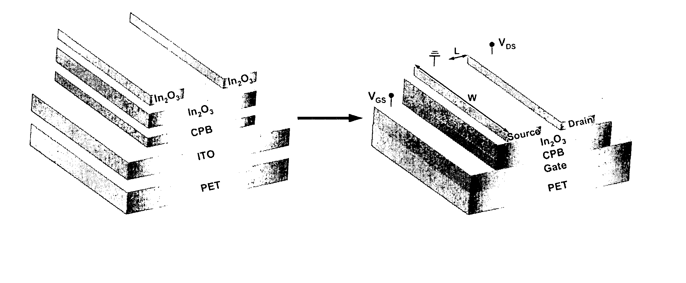
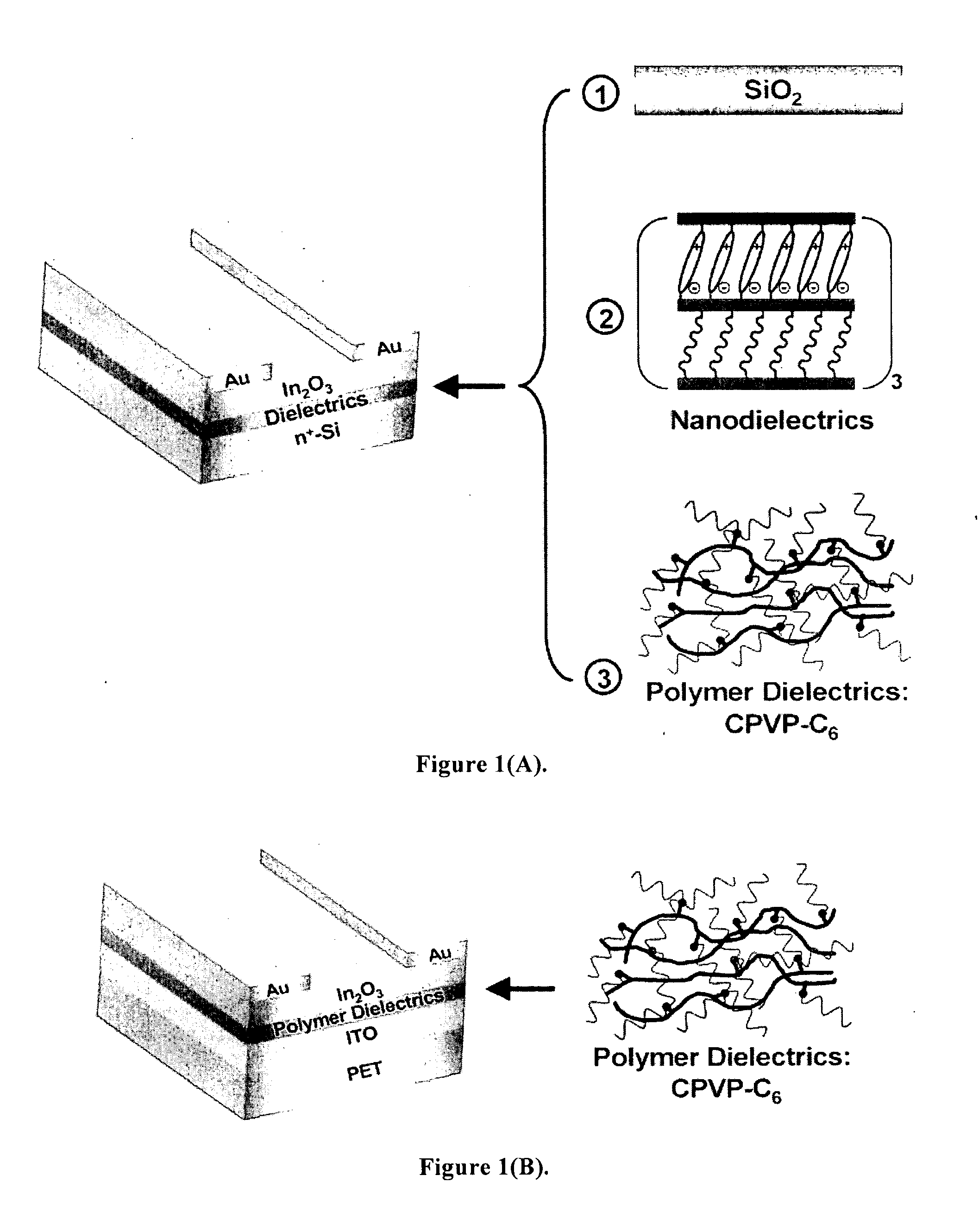
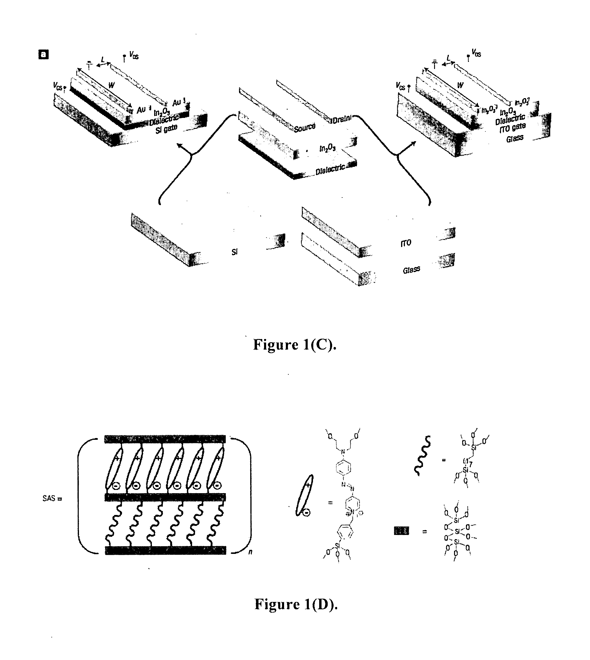
[0073] TFT Fabrication. In2O3 thin films were deposited on p+-Si / SiO2 (Process Specialties, Inc.), n+-Si / (SAS nanodielectric) (n+-Si from Process Specialties, Inc.), n+-Si / (crosslinked polymer blend dielectric), and PET / ITO / (crosslinked polymer blend dielectric) (ITO / PET, (Rsheet=80 Ω / □), from CPFilms Inc.), and IAD-derived glass / ITO (Corning 1737F glass substrates from Precision Glass & Optics; the ITO gate was deposited by IAD at room temperature; sheet resistance=60 Ω / □) as the back gate. The nanoscopic organic gate dielectrics (SAS, three 5.5 nm layers of type III; CPB, 20 nm prepared from poly-4-vinylphenol+1,6-bis(trichlorosilyl)hexane) were grown via layer-by-layer self-assembly or spin-coating, as provided in the references incorporated herein. Poly-4-vinylphenol and 1,6-bis(trichlorosilyl)hexane were purchased from Aldrich and Gelest, respectively.
[0074] In2O3films were grown with a Veeco horizontal dual-gun IAD system at room temperature. The In2O3 target (99.99%) was pur...
example 2
[0076] Characterization. In2O3 film thicknesses were verified using a Tencor P-10 step profilometer by etching a step following film growth. XRD θ-2θ scans of In2O3 were acquired with a Rigaku DMAX-A diffractometer using Ni-filtered Cu Kα radiation. Optical transmittance spectra were acquired with a Cary 500 ultraviolet-visible-near-infrared spectrophotometer and were referenced to the spectrum of uncoated Corning 1737F glass. Film surface morphologies were imaged on a Digital Instruments Nanoscope III AFM. Quantitative SIMS analysis was carried out on a MATS quadrupole SIMS instrument using a 15 keV Ga+ ion source. Conductivities of the semiconducting In2O3 thin films were measured with a Keithley 2182A nanovoltmeter and 6221 current source. The electrical properties of highly conductive ITO and In2O3 films were characterized on a Bio-Rad HL5500 van der Pauw Hall-effect measurement system. TFT device characterization was carried out on a customized probe station in air with a Keith...
example 3
[0077] TFTs fabricated with another inorganic n-channel semiconductor, ZnO, are demonstrated on inorganic SiO2 dielectrics. For instance, ZnO films were deposited on p+-Si / SiO2(300 nm) substrates at room temperature by ion-assisted deposition (IAD). The ZnO thin film growth conditions were similar to those of In2O3, above. The energies (currents) used to produce the primary and assisted ion beams were 180 W(186 mA) and 75 W(37 mA), respectively. The system growth pressure and O2 partial pressure were 2.8×10⁻⁴˜3.0×10⁻⁴ Torr and 0.5×10⁻⁴˜0.8×10⁻⁴ Torr, respectively. The growth rate of ZnO thin films was 4.1±0.1 nm / min. All ZnO TFTs were fabricated at room temperature. The ZnO films exhibited clear field-effect n-type response. Details of such ZnO TFT characteristics are shown in FIGS. 13-14. In particular, ZnO TFTs fabricated on p+-Si / SiO2 substrates exhibit typical field-effect I-V characteristics (FIG. 13A) with classical linear and pinch-off saturation lines. ZnO TFTs show a field-...
PUM
 Abstract
Description
Claims
Application Information