Insulating film formation method, semiconductor device, and substrate processing apparatus

a technology of substrate processing and film formation method, which is applied in the direction of polycrystalline material growth, natural mineral layered products, crystal growth process, etc., can solve the problems of insulating film thickness differences, and achieve good thickness uniformity, good thickness uniformity, and good thickness uniformity.

Active Publication Date: 2008-01-31
PANNOVA SEMIC
View PDF4 Cites 14 Cited by
  • Summary
  • Abstract
  • Description
  • Claims
  • Application Information

AI Technical Summary

Benefits of technology

[0020]With the substrate processing apparatus, the first material gas more highly reactive than the second material gas is supplied from the first nozzle. Then, the highly reactive first material gas supplied flows onto each of the substrates in the form of a laminar flow. Therefore, variations in the flow rate of the first material gas supplied onto the substrate can be reduced to provide an insulating film with a good thickness uniformity. Moreover, the first nozzle can have a gas supply orifice with an increased diameter as compared with the holes formed in the second nozzle. Therefore, even in the case where a gas more highly reactive than the second material gas is used as the first material gas, the occurrence of particles as reaction products can be suppressed. This prevents the particles blown up by a turbulent flow from adhering onto the substrates and the like. As a result of this, the substrate processing apparatus according to the present invention can form an insulating film with a good thickness uniformity and a good film composition uniformity within the substrate.
[0021]Preferably, in the substrate processing apparatus according to the present invention, each of the plurality of holes is arranged in shifted relation to the same direction as the direction of rotation of the wafer boat so that the angle formed between: a straight line connecting the central axis of the second nozzle on a cut surface thereof in parallel with the principal plane of the substrate and the central axis of the substrates; and a straight line connecting the central axis of the second nozzle and the center of each said hole ranges from 5° to 90° inclusive. This enables supply of the second material gas even onto the center portion of the substrate, so that film thickness variations within the substrate such that the film thickness is greater at the edge portion of the substrate and smaller at the center portion thereof can be reduced to provide an insulating film with an excellent thickness uniformity within the substrate.

Problems solved by technology

This causes the problem that the difference in the insulating film thickness occurs or the film compositions of the insulating films vary between wafers disposed in an upper area and a lower area of the reaction tube.

Method used


Image

  • Insulating film formation method, semiconductor device, and substrate processing apparatus
  • Insulating film formation method, semiconductor device, and substrate processing apparatus
  • Insulating film formation method, semiconductor device, and substrate processing apparatus

Examples


first embodiment

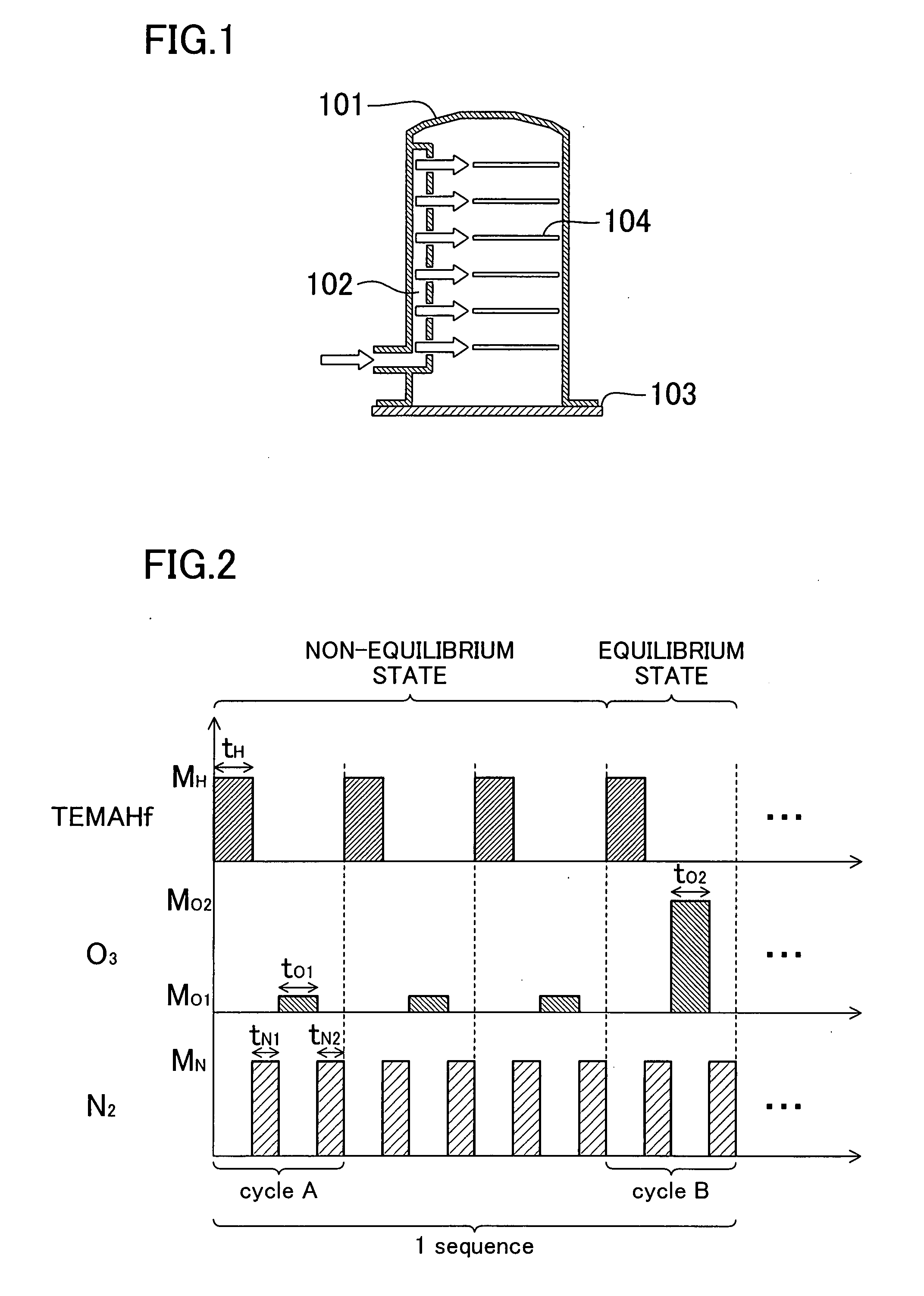
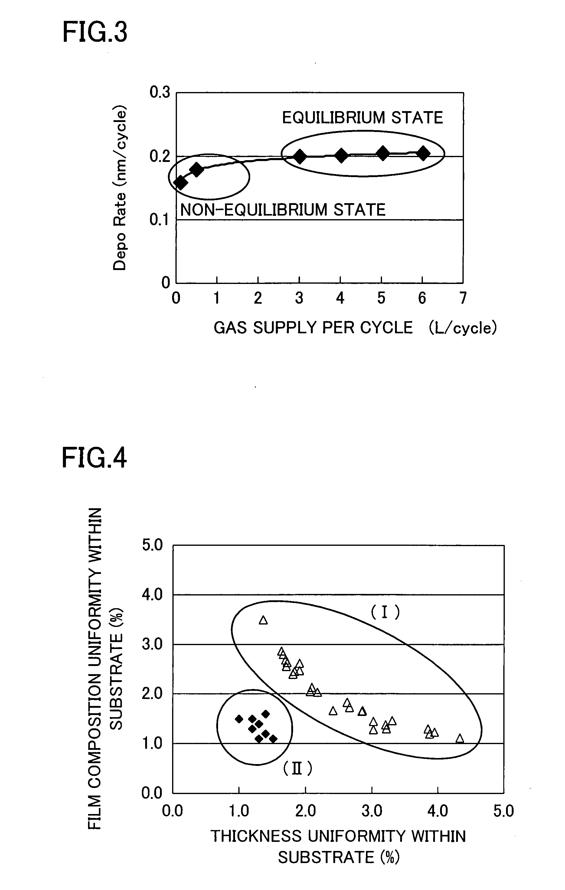
[0034]An insulating film formation method according to a first embodiment of the present invention will be described below with reference to the accompanying drawings. This description will be made exemplarily using formation of a capacitor insulating film made of a hafnium oxide film.

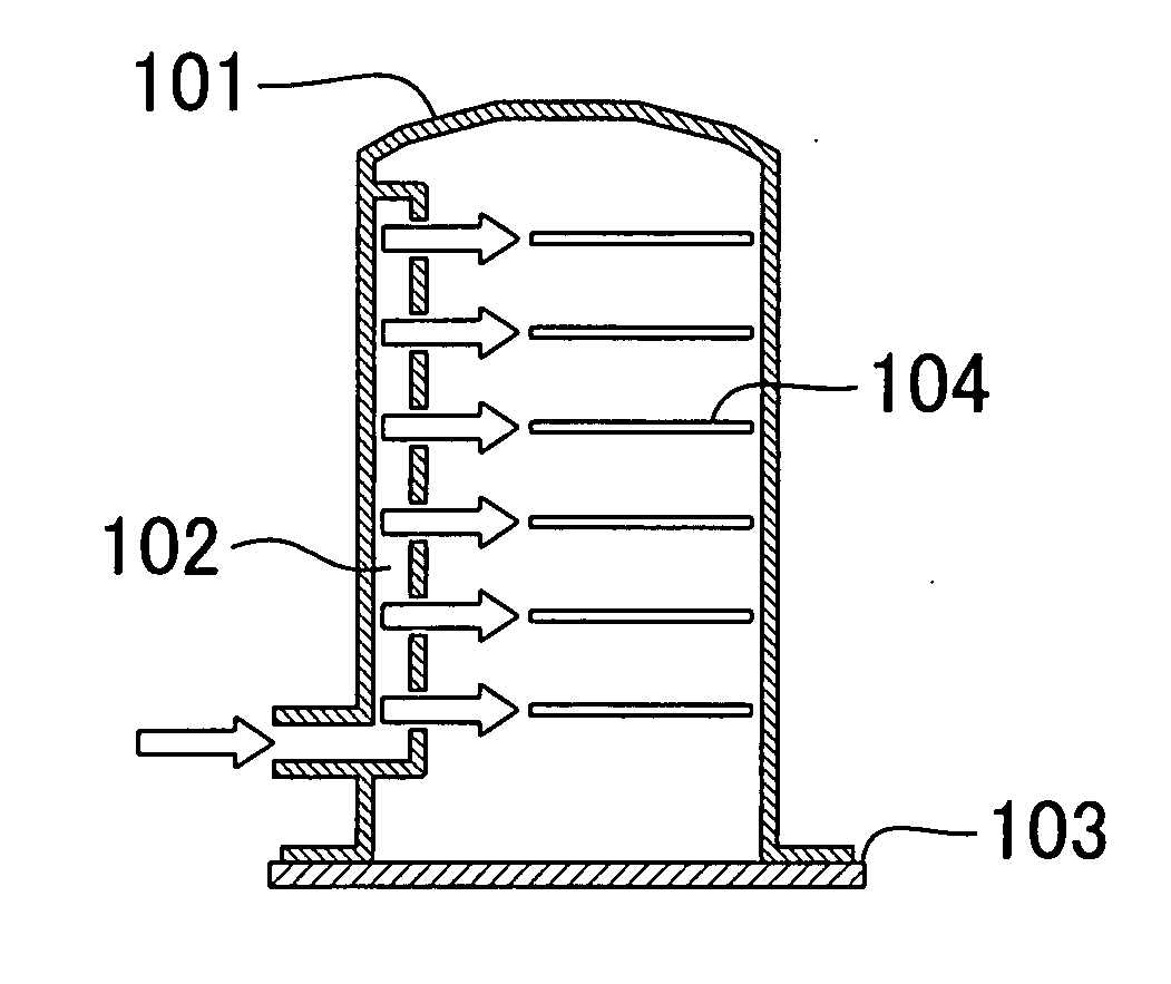
[0035]FIG. 1 is a sectional view showing the structure of a substrate processing apparatus (referred hereinafter to as a first vertical batch ALD apparatus) used in the insulating film formation method according to the first embodiment of the present invention.

[0036]Referring to FIG. 1, the first vertical batch ALD apparatus includes: a reaction chamber 101; a wafer boat (not shown); and a plurality of first nozzles 102. The reaction chamber 101 is used to form an insulating film on each of multiple substrates 104. The wafer boat is used to mount the multiple substrates 104 so that they are aligned at given intervals in the perpendicular direction of the reaction chamber 101. The first nozzles 102 exte...

second embodiment

[0062]An insulating film formation method and a substrate processing apparatus according to a second embodiment of the present invention will be described below with reference to the accompanying drawings. This description will be made exemplarily using formation of a capacitor insulating film made of a hafnium oxide film. FIG. 5 is a sectional view showing the structure of a substrate processing apparatus (referred hereinafter to as a second vertical batch ALD apparatus) according to the second embodiment of the present invention.

[0063]Referring to FIG. 5, the second vertical batch ALD apparatus includes: a reaction chamber 101; a wafer boat (not shown); a plurality of first nozzles 102; and a second nozzle 201. The reaction chamber 101 is used to form an insulating film on each of multiple substrates 104. The wafer boat is used to mount the multiple substrates 104 so that they are aligned at given intervals in the perpendicular direction of the reaction chamber 101. The first nozz...

third embodiment

[0091]A substrate processing apparatus according to a third embodiment of the present invention will be described below with reference to the accompanying drawings. The substrate processing apparatus of the third embodiment (referred hereinafter to as a third vertical batch ALD apparatus) has the structure in which holes provided in a first nozzle are arranged at different positions from those of the first vertical batch ALD apparatus of the first embodiment. FIG. 9 is a top view partly showing the structure of the substrate processing apparatus according to the third embodiment of the present invention.

[0092]Referring to FIG. 9, the third vertical batch ALD apparatus includes: a reaction chamber 101 (not shown); a wafer boat (not shown); and a plurality of first nozzles 102. The reaction chamber 101 is used to form an insulating film on each of multiple substrates 104. The wafer boat is used to mount the multiple substrates 104 so that they are aligned at given intervals in the per...


PUM

PropertyMeasurementUnit
angleaaaaaaaaaa
thicknessaaaaaaaaaa
pressureaaaaaaaaaa

Abstract

In an insulating film formation method, a cycle A in which O3 at a low flow rate is supplied onto a substrate and then O3 supplied is allowed to react with Hf on the substrate in a non-equilibrium state to form a hafnium oxide film is carried out M times (M≧1), and a cycle B in which O3 at a high flow rate is supplied onto the substrate and then O3 supplied is allowed to react with Hf on the substrate in an equilibrium state to form a hafnium oxide film is carried out N times (N≧1). These insulating film formation cycles are defined as one sequence. This sequence is repeated until a desired thickness is obtained, thereby forming a target insulating film.

Description

BACKGROUND OF THE INVENTION[0001](a) Fields of the Invention[0002]The present invention relates to insulating film formation methods employed for semiconductor devices, semiconductor devices, and substrate processing apparatus.[0003](b) Description of Related Art[0004]In recent years, the wafer size of a semiconductor substrate has been enlarged and a semiconductor element design has become finer. With such trend, decreasing variations in processing dimensions among apparatus for mass production becomes important in order to improve the fabrication yield thereof. In particular, since the thickness uniformity of a gate insulating film or a capacitor insulating film affects variations in the characteristics of a device using this insulating film, it is desirable that the thickness uniformity of the insulating film, such as the uniformity within a wafer, the wafer-to-wafer uniformity, and the process-to-process uniformity, be good.[0005]Since a device with a design rule of 100 nm or sm...

Claims


Application Information

Patent Timeline
Patent Type & Authority Applications(United States)
IPC IPC(8): H01L21/31B32B9/00C23C16/00
CPCC23C16/405C23C16/45504C23C16/45546H01L21/02164H01L21/0217H01L21/3185H01L21/0228H01L21/3141H01L21/31608H01L21/31645H01L21/02181
Inventor SUZUKI, JUNYONEDA, KENJIMATSUYAMA, SEIJI
Owner PANNOVA SEMIC
Why Eureka
Try Eureka