Method Of Treating The Surface Of Copper And Copper

a technology of surface treatment and copper, applied in the direction of solid-state diffusion coating, superimposed coating process, transportation and packaging, etc., can solve the problems of reduced adhesion between the surface of copper and the resist pattern, difficulty in obtaining the accuracy of the resist pattern, and peeled resist pattern

Active Publication Date: 2008-04-24
RESONAC CORP
View PDF5 Cites 40 Cited by
  • Summary
  • Abstract
  • Description
  • Claims
  • Application Information

AI Technical Summary

Benefits of technology

[0018] Moreover, the variation in the height of the irregularities is large and when Rz<0.5 μm, there is the problem that reliability of the adhesion under high temperature and high humidity condition is reduced whereas when Rz>1.0 μm, there is the problem that the transfer loss is increased in the same manner as in the first prior technologies. Also, because needle crystals of copper oxide are easily broken, and flat line treatment cannot be performed, posing a problem concerning deteriorated operability when a thin plate is treated. Moreover, in a plating process for connecting a through-hole, the needle crystals of copper oxide are dissolved whereby a pink color ring (pink ring) is generated in the vicinity of the through-hole with the result that the reliability to insulation is easily deteriorated and the surface of copper is easily peeled from the insulating resin. Also, since a high-temperature aqueous alkaline solution is used, the surface of the insulating resin is easily affected and the reliability to insulation tends to be reduced by ionic contamination or a deterioration in insulation. In addition, there is the problem that in the washing with water after oxidation treatment, the space between needle crystals can be insufficiently washed with water because of complicated needle crystal irregularities of copper oxide and the reliability to insulation is therefore easily reduced by residual ions present between crystals.
[0020] It is an object of the present invention, which is made to improve the above prior art problems, to provide a method of treating the surface of copper, the method securing the adhesive strength between the surface of copper and a resist or an insulating resin without forming irregularities exceeding 1000 nm on the surface of copper, ensuring that various kinds of reliability can be improved and also to provide copper whose surface is treated by the above surface treating method.
[0034] According to the present invention as mentioned above, it is possible to provide a method of treating the surface of copper, the method securing the adhesive strength between the surface of copper and a resist or an insulating resin without forming irregularities exceeding 1000 nm on the surface of copper, ensuring that various kinds of reliability can be improved and also to provide copper whose surface is treated by the above surface treating method.

Problems solved by technology

However, there is the problem that in the formation of fine wiring having L / S of 30 μm / 30 μm or less, it is difficult to obtain accuracy of a resist pattern by the influence of halation caused by the reflection of light on the shiny surface of copper when the resist is exposed to light.
Also, there is the problem that the adhesion between the surface of copper and the resist pattern is reduced with the result that the resist pattern is peeled off.
There is also the problem that the adhesion between the wiring (copper) and the solder resist and between the wiring and the cover lay, on the other hand, is insufficiently obtained as the wiring is more fined.

Method used


Image

  • Method Of Treating The Surface Of Copper And Copper
  • Method Of Treating The Surface Of Copper And Copper
  • Method Of Treating The Surface Of Copper And Copper

Examples


example 1

[0146] Semiconductor package samples were manufactured in the following manner to evaluate the reliability of a semiconductor package manufactured by applying the copper surface treatment of the present invention.

[0147] (Step a)

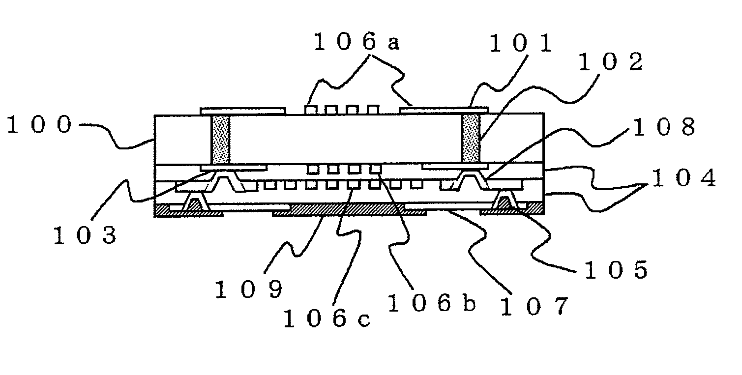
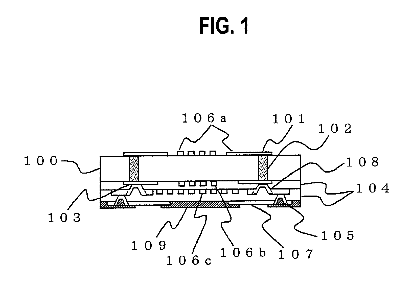
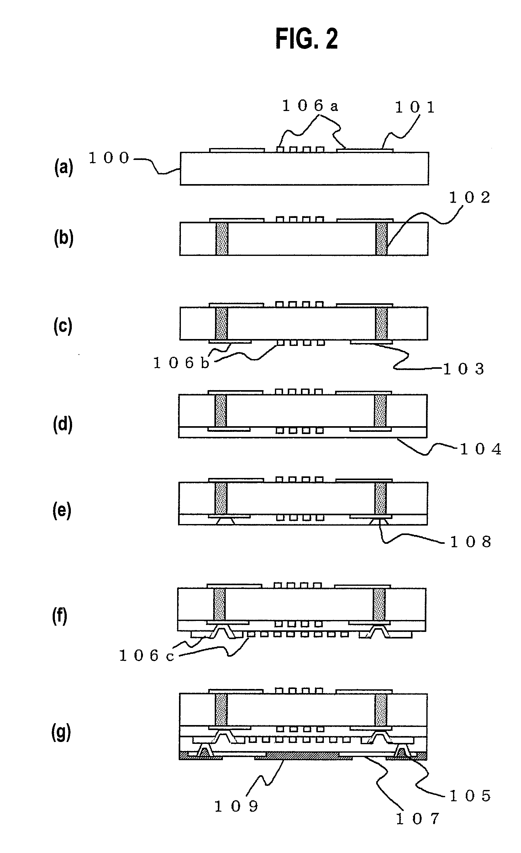
[0148] A soda glass substrate (thermal expansion coefficient: 11 ppm / ° C.) of 0.4 mm in thickness was prepared as a core substrate 100. A 200 nm-thick copper thin film was formed on one surface of the substrate by sputtering, and then electroplated with copper to a thickness of 10 μm. The sputtering was carried out using an apparatus (model No. MLH-6315, manufactured by Ulvac, Inc.) in the following condition 1.

Condition 1

[0149] Current: 3.5 A

[0150] Voltage: 500 V

[0151] Flow rate of argon: 35 SCCM (0.059 Pa·m3 / s)

[0152] Pressure: 5×10⁻³ Torr (6.6×10⁻¹ Pa)

[0153] Film formation speed: 5 nm / sec.

[0154] Then, an etching resist was formed on the part to be a first wiring 106a and then the copper layer was etched by a ferric chloride etching solution and th...

example 2

[0189] A fan-in type substrate for mounting a semiconductor chip for BGA and a semiconductor package were manufactured in the same manner as in Example 1 except that a reducing process was carried out, the process including washing the surface of the second wiring 106b with water for 5 minutes, dipping the substrate at 40° C. for 3 minutes in a reducing process solution HIST-100D (trade name, Hitachi Chemical Co., Ltd.), washing further with water for 10 minutes and drying at 85° C. for 30 minutes, after copper oxide crystals were formed on the surface of the second wiring 106b in the (step d-2) and before the buildup layer 104 was formed in the (step d-3).

example 3

[0190] A fan-in type substrate for mounting a semiconductor chip for BGA and a semiconductor package were manufactured in the same manner as in Example 1 except that a coupling process was carried out, the process including washing the surface of the second wiring 106b with water for 5 minutes, dipping the substrate at 30° C. for 3 minutes in an aqueous solution containing 0.5% by weight of γ-aminopropyltriethoxysilane, washing further with water for 1 minute and drying at 85° C. for 30 minutes, after copper oxide crystals were formed on the surface of the second wiring 106b in the (step d-2) and before the buildup layer 104 was formed in the (step d-3).


PUM

PropertyMeasurementUnit
roughness Rzaaaaaaaaaa
heightaaaaaaaaaa

Abstract

A method of treating the surface of copper is provided to ensure adhesive strength between the surface of copper and an insulating layer without forming irregularities exceeding 1 μm on the surface of copper and to improve insulation reliability between wirings. A copper whose surface is treated by the above surface treating method is also provided. The method of treating the surface of copper comprises the surface of copper comprising the steps of: forming a metal nobler than copper discretely on the surface of copper; and subsequently oxidizing the surface of copper by using an alkaline solution containing an oxidant.

Description

FIELD OF THE INVENTION [0001] The present invention relates to a method of treating the surface of copper and to copper which is surface-treated by the surface treating method. BACKGROUND ART [0002] The recent information-oriented society has been remarkably developed. Along with this, small-sized, light-weight, high performance and high functional devices such as personal computers and portable telephones for public use are being developed and there is also a current need for an improvement in radio base stations, optical communication devices and relevant network devices such as servers and routers for industrial use irrespective of size. And, with an increase in the amount of information to be transferred, frequency of signals to be handled are becoming higher year by year and developments in high-speed processing and high-speed transfer technologies are being made. With regard to the packaging concerned, system-on-chip (SoC), system-in-package (SiP) and the like are being develo...

Claims


Application Information

Patent Timeline
Patent Type & Authority Applications(United States)
IPC IPC(8): C23F1/00B32B15/20
CPCC23C8/02Y10T428/12771C23C22/63C23C28/00H05K3/384H05K3/385H05K3/389H05K3/4644H05K2201/0347H05K2201/0373H05K2203/0315H05K2203/1157C23C8/40Y10T428/24917Y10T428/12875Y10T428/12438C23C28/321C23C28/322C23C28/345H01L2224/48091H01L2224/73204H01L2224/73265H01L2924/15311H01L2224/45144Y10T428/12993Y10T428/12903H01L2924/00014H01L2924/00H01L2224/16225H01L2224/32225H01L2924/181H01L2924/00012C23C22/68C23C22/78C23C22/83
Inventor YAMASHITA, TOMOAKIINOUE, YASUOMATSUURA, MASAHARUITO, TOYOKISHIMIZU, AKIRAINOUE, FUMIONAKASO, AKISHI
Owner RESONAC CORP
Why Eureka
Try Eureka