Semiconductor device and method of fabricating the same

a technology of semiconductor devices and semiconductor devices, applied in semiconductor devices, semiconductor/solid-state device details, electrical apparatus, etc., can solve problems such as junction leakage or spike, occurrence of threshold voltage (vth) shift, and recent vanishing of contact plugs as wiring resistance elements

Inactive Publication Date: 2008-05-01
KK TOSHIBA
View PDF3 Cites 40 Cited by
  • Summary
  • Abstract
  • Description
  • Claims
  • Application Information

AI Technical Summary

Benefits of technology

[0012] In another aspect, the invention provides a semiconductor device comprising a semiconductor substrate including an upper surface, a polycrystalline silicon layer formed on the upper surface of the semiconductor substrate, an insulating film formed on the polycrystalline silicon layer, and a contact plug formed in the insulating film so that the contact plug electrically contacts with the polycrystalline

Problems solved by technology

With miniaturization of devices and increase in an operating speed of a semiconductor device, the resistance of the contact plug as an element of wiring resistance has recently been rendered so large as to be unignorable.
As a result, the operating speed of the semiconductor device has adversely been affected by the increased resistance of the contact plug.
Consequently, each of aluminum and copper as impurity forms an interface state on a bo

Method used


Image

  • Semiconductor device and method of fabricating the same
  • Semiconductor device and method of fabricating the same
  • Semiconductor device and method of fabricating the same

Examples


first embodiment

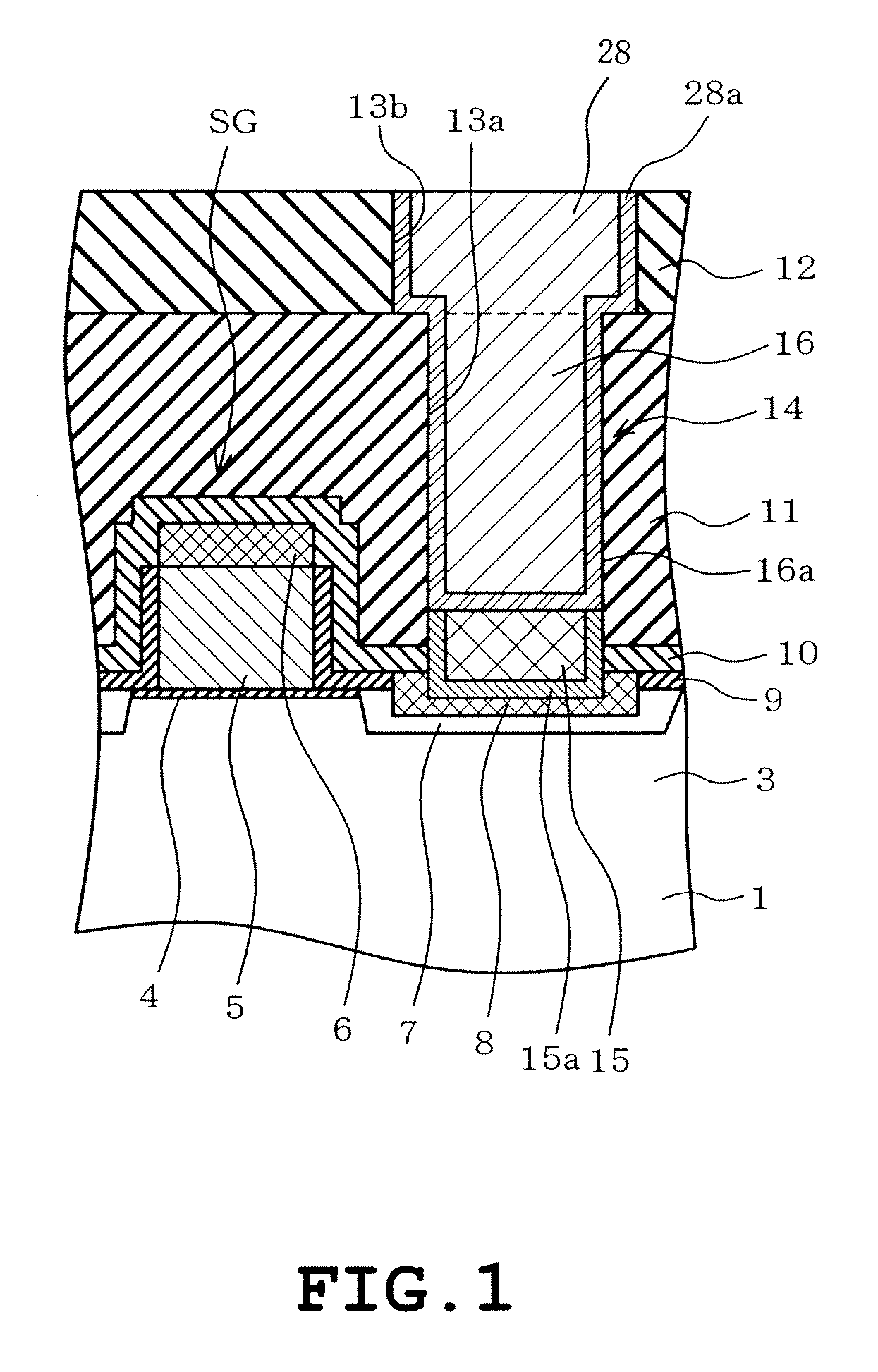
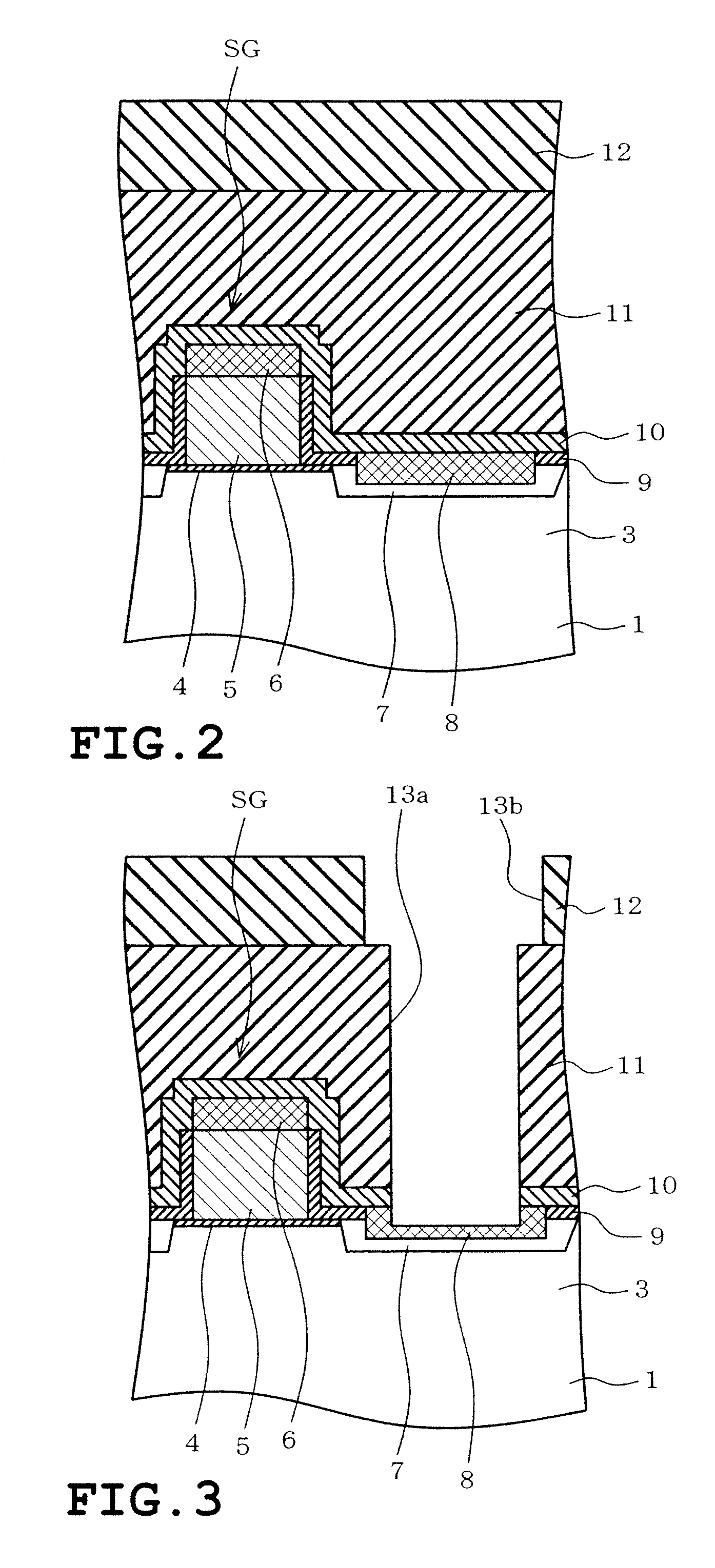
[0025]FIG. 1 is a sectional view of a contact of the semiconductor device of a A semiconductor substrate 1 includes an active area 3 on which a gate electrode SG is formed. The gate electrode SG is comprised of a tunnel insulating film 4 formed on the semiconductor substrate 1. A polycrystalline silicon film 5 and a cobalt silicide film 6 are deposited on the tunnel insulating film 4 in turn. Two source / drain regions 7 one of which is shown are formed at both sides of the gate electrode SG respectively. Each source / drain region 7 serves as an impurity diffusion region and is formed by introducing impurities into a surface layer of the substrate 1 by an ion implantation. A cobalt silicide layer 8 is formed on a surface of the source / drain region 7.

[0026] A silicon oxide film 9 is formed on a sidewall of the gate electrode SG and the surface of the source / drain region 7 by a rapid thermal processing (RTP) or the like so as to reach a predetermined height with respect to the surface o...

fourth embodiment

[0047] In the fourth embodiment, the thin film ruthenium layer is used as the copper barrier metal layer 16a, and the direct plating method necessitating no copper seed is used. Accordingly, the above-described method can cope with refinement of design rules. Consequently, a larger opening diameter of the contact hole 13a before copper plating can be ensured as compared with the method of forming the barrier metal layer and copper seed with the use of PVD method. Copper can be buried even when the method is applied to microscopic contacts.

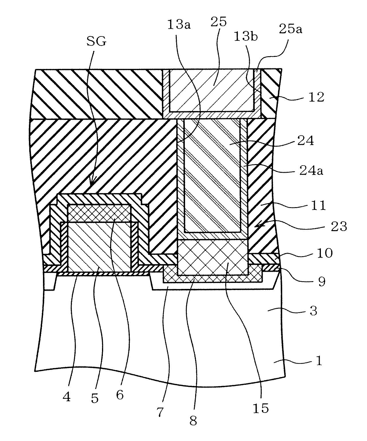
[0048]FIG. 14 illustrates a fifth embodiment of the invention. The fifth embodiment differs from the fourth embodiment in that the contact plug 23 and the interlayer wiring 25 are separate from each other. In the fourth embodiment, the copper layer is formed simultaneously on the contact hole 13a and the groove 13b, whereby the contact plug 22 and the interlayer wire are formed. Thus, the fabrication process employs the dual damascene method in the...


PUM


Abstract

A semiconductor device includes a semiconductor substrate including an impurity diffusion region within an upper surface thereof, an insulating film formed on an upper surface of the impurity diffusion region, and a contact plug formed in the insulating film so that the contact plug contacts the impurity diffusion region. The contact plug includes a first conductor layer contacting the upper surface of the impurity diffusion region and a second conductor layer formed on the first conductor layer including copper (Cu) or copper alloy layers, and the first conductor layer including a material which suppresses diffusion of the copper of the second conductor layer to the semiconductor substrate.

Description

CROSS-REFERENCE TO RELATED APPLICATIONS [0001] This application is based on and claims the benefit of priority from the prior Japanese Patent Application No. 2006-297828, filed on Nov. 1, 2006, the entire contents of which are incorporated herein by reference. BACKGROUND OF THE INVENTION [0002] 1. Field of the Invention [0003] The present invention relates to a semiconductor device provided with contact plugs electrically connecting a transistor source, drain or a gate to a first layer wire and a method of fabricating the same. [0004] 2. Description of the Related Art [0005] Semiconductor devices such as memory devices and logic devices have conventionally been provided with contact plugs which electrically connect a transistor source, drain or gate to first layer wirings including tungsten (W), aluminum (Al) and copper (Cu) wirings. The contact plugs are formed on a silicon substrate on which sources, drains or gates are formed, a silicide layer or a polycrystalline silicon layer. ...

Claims


Application Information

Patent Timeline
IPC IPC(8): H01L23/52H01L21/4763
CPCH01L21/76807H01L21/76847H01L21/76877H01L21/76879H01L23/485H01L2924/0002H01L23/53238H01L2924/00
Inventor KATATA, TOMIO
Owner KK TOSHIBA
Why Eureka
Try Eureka