

Process and system for laser annealing and laser-annealed semiconductor film
- Summary
- Abstract
- Description
- Claims
- Application Information
AI Technical Summary
Benefits of technology
Problems solved by technology
Method used
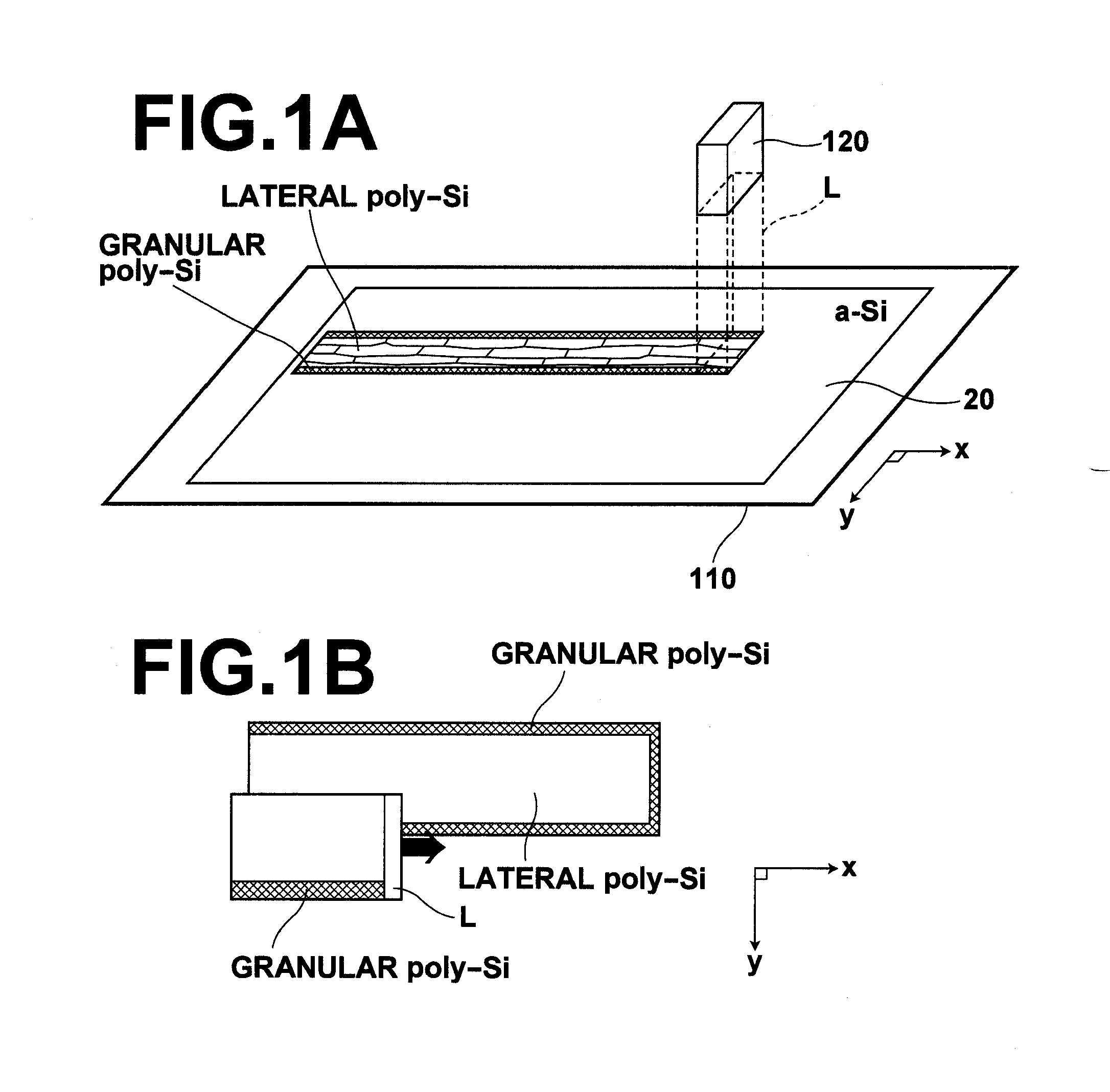
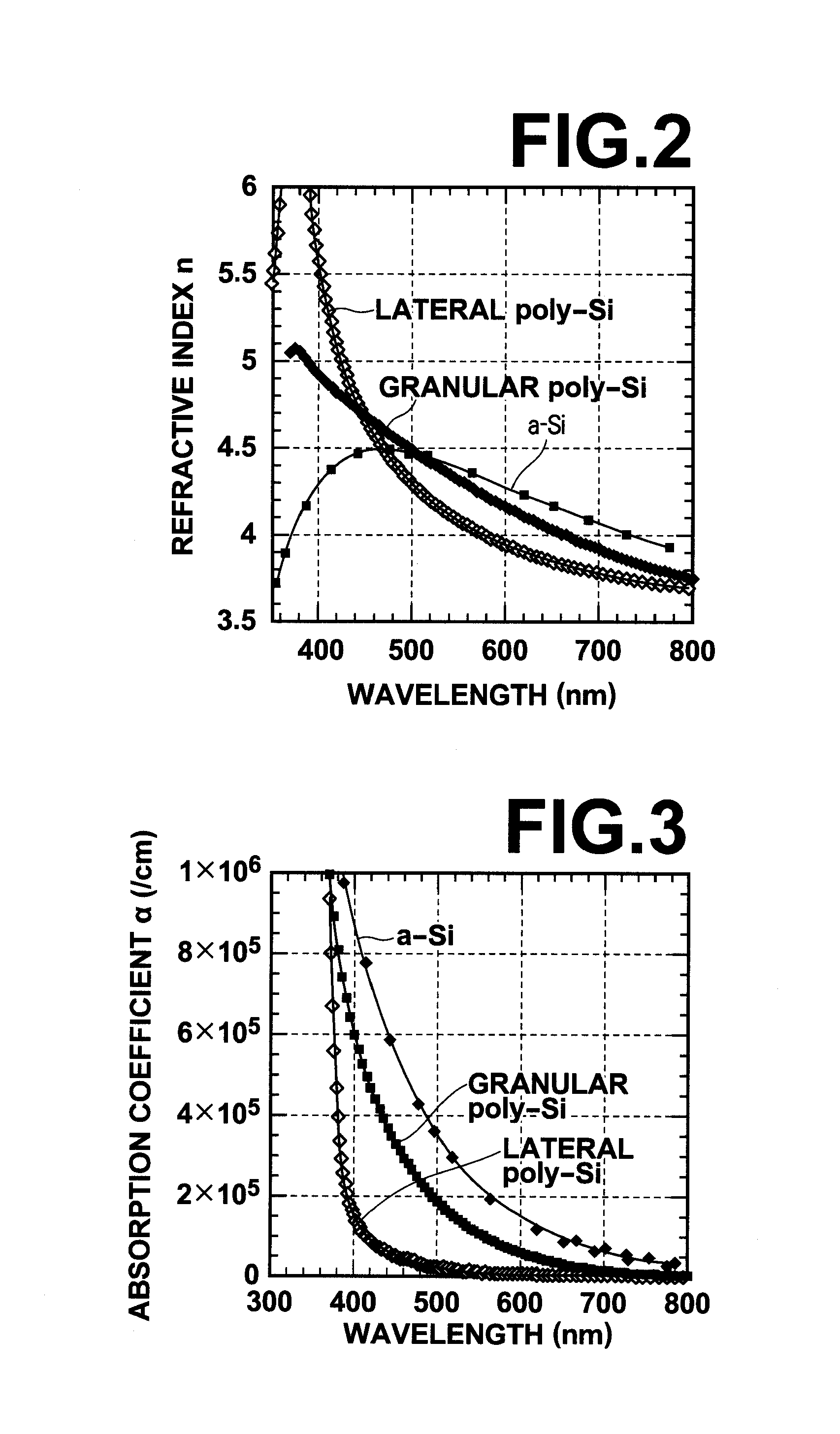
Image

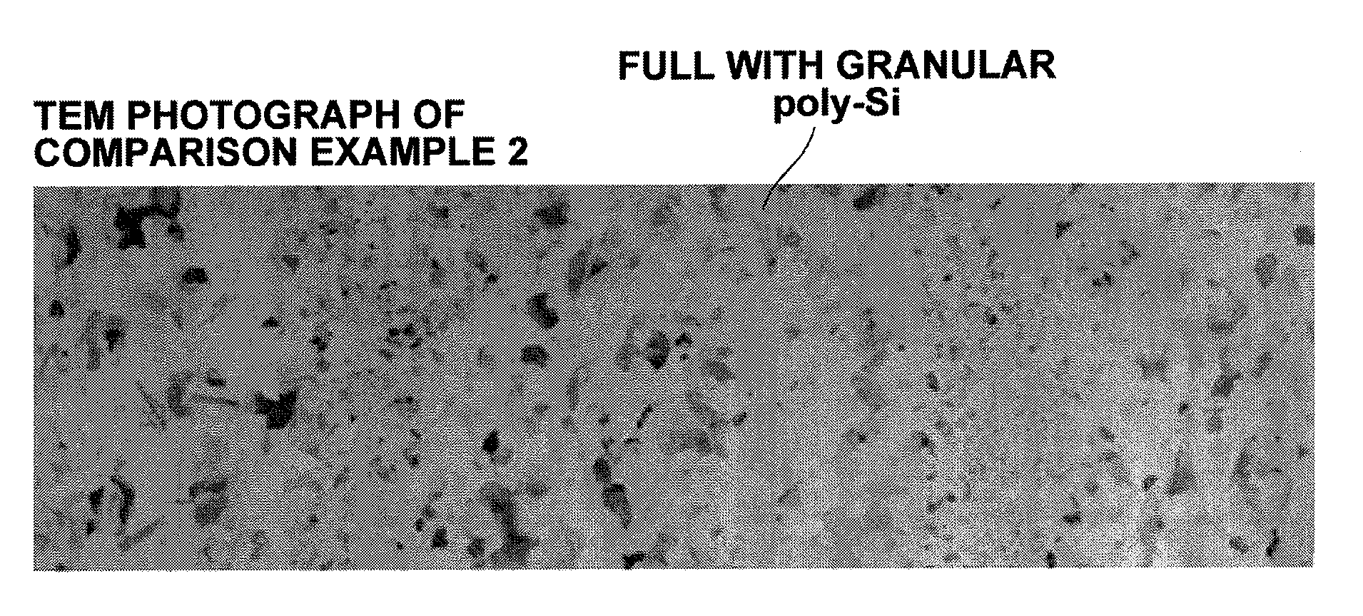
Examples
concrete example 1
[0208] A concrete example 1 of the semiconductor film according to the present invention has been produced in accordance with the following procedure.
[0209] A bedding layer of silicon oxide having a thickness of 20 nm and a noncrystalline silicon (a—Si) film having a thickness of 50 nm are formed in this order on a glass substrate by plasma CVD. Thereafter, heat annealing is performed at approximately 500° C. for approximately 10 minutes, and dehydrogenation of the noncrystalline silicon film is performed.
[0210] Next, laser annealing of the noncrystalline silicon film is performed by using the laser annealing system 100 as illustrated in FIGS. 10 and 11, where GaN-based semiconductor lasers having the oscillation wavelength of 405 nm are used in the laser-light source, and the laser beam L has an elongated rectangular cross section with the dimensions of 20×3 micrometers at the surface of the noncrystalline silicon film. The noncrystalline silicon film has been substantially entir...
PUM
 Abstract
Description
Claims
Application Information