Method of making a variable resistance memory

Inactive Publication Date: 2008-05-08
SYMETRIX
View PDF8 Cites 143 Cited by
  • Summary
  • Abstract
  • Description
  • Claims
  • Application Information

AI Technical Summary

Benefits of technology

[0011]The invention solves the above and other problems by providing methods for making resistive switching materials, generally called variable resistance materials (VRM) in the art, memories utilizing such materials, and integrated circuits utilizing the materials. In particular, chemical solution deposition (CSD) methods, preferably utilizing a metallorganic or organometallic precursor, and most preferably, having octane as a solvent, are disclosed. CSD methods include spin-on, misted deposition, metallorganic chemical vapor deposition (MOCVD), dipping, and atomic layer deposition (ALD). Preferably, the chemical solution provides the element carbon. These methods preferably include a reaction in a gas containing the extrinsic ligand elements that stabilize the VRM or a gas containing the anion to which the ligand bonds, or both. The reaction may take place in an anneal process in a gas containing the ligand, the anion, or both; or the reaction may take place in a reactive sputtering in a gas containing the ligand, the anion, or both.
[0012]The invention provides a method of making a resistive switching integrated circuit memory, said method comprising: providing a substrate and a metallorganic or organometallic precursor including a metal moiety suitable for forming a desired variable resistance material (VRM); applying said precursor to said substrate to form a thin film of said precursor; heating said precursor on said substrate to form said VRM; and completing said integrated circuit to include said VRM as an active element in said integrated circuit. Preferably, said precursor comprises octane. Preferably, said applying comprises a process selected from the group consisting of: spin-coating, dipping, liquid source misted deposition, chemical vapor deposition, and atomic layer deposition. Preferably, said heating comprises annealing in oxygen. Preferably, said heating comprises annealing in a gas containing at least one chemical element for forming a ligand which stabilizes the electronic properties of said VRM. Preferably, said gas comprises a gas selected from CO and CO2. Preferably, said annealing comprises annealing in a gas containing the an

Problems solved by technology

Once these devices left the factory, they could not be re-written.
However, the worse limiting factor is the limited number of erase/write cycles to no more than slightly over 600,000—or of the order of 105-106.
FeRAMs (Ferroelectric RAMs) provide low power, high write/read speed, and endurance for read/write cycles exceeding 10 billion times. Magnetic memories (MRAMs) provide high write/read speed and endurance, but with a high cost premium and higher power consumption.
However, it is generally recognized that Flash will not scale easily below 65 nanometers (nm); thus, new non-volatile memories that will scale to smaller sizes are actively being sought.
However, these resistance-based memories have not proved to be commercially successful because their transition from the conductive to the insulating state depends on a physical structure phenomenon, i.e., melting (at up to 600° C.) and returning to a solid state that cannot be sufficiently controlled for a useful memory.
However, no examples of fabrication of actual devices is given.
Further, none demonstrate conductive and insulative states that are stable over the necessary temperature range and which do not fatigue over many memory cycles.
In relation to varia

Method used


Image

  • Method of making a variable resistance memory
  • Method of making a variable resistance memory
  • Method of making a variable resistance memory

Examples


example i

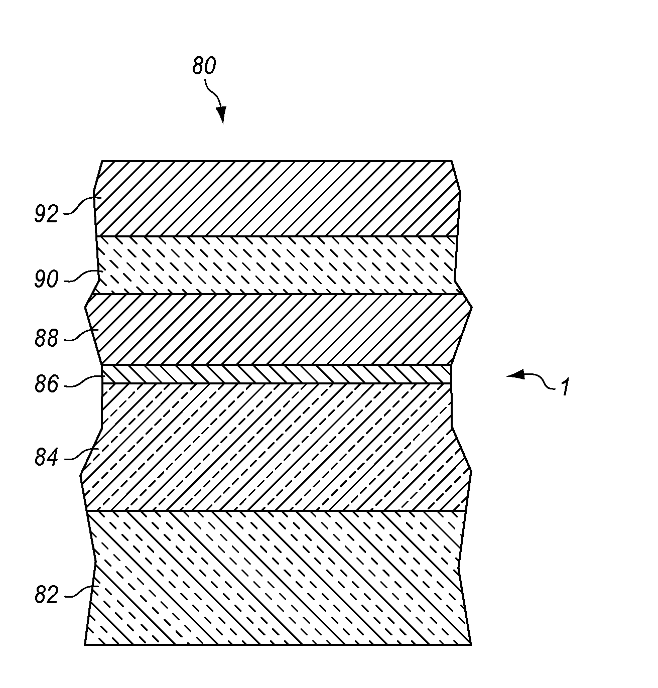
[0040]A 2000 Å (Angstrom) layer of platinum was deposited on a wafer with a silicon dioxide coating. Then a 0.2 molar nickel oxide precursor in an octane solution was deposited by spin coating the platinum layer at 3000 rpm (rounds per minute). The nickel oxide precursor is available from Kojundo Chemical Company, Tokyo, Japan. The precursor was baked at 150° C. for 1 minute, and then at 260° C. for four minutes to produce an approximately 100 Å dry layer. The spin-on deposition and baking processes were repeated six times for a total thickness of 600 Å. Then a crystallization anneal was performed in a furnace at 450° C. in an oxygen atmosphere for 40 minutes to produce a 600 Å layer of the VRM nickel oxide according to the invention. Electron microscopy revealed that a significant amount of carbon was present in the material, with the carbon coming from the octane precursor. Since both a metallorganic precursor and an organometallic precursor contain carbon, either precursor can be...

example ii

[0041]This example was made in the same way as Example I above except that 5% ammonia was added to the precursor. The films produced yielded similar results.

[0042]The invention includes an annealing process for VRMs. The VRM may be annealed in a gas containing at least one chemical element for forming a ligand which stabilizes the electronic properties of the VRM. Preferably, the VRM is a transition metal and the chemical element comprises carbon. Preferably, the gas comprises a gas selected from CO and CO2. Preferably, the VRM is nickel.

[0043]The invention also provides a sputtering method of making a VRM. The material may be sputtered and then annealed as described above; or reactive sputtering of the VRM in a gas containing at least one chemical element for forming a ligand which stabilizes the electronic properties of the VRM may be employed. Preferably, the VRM is a transition metal and the chemical element comprises carbon. Preferably, the gas comprises a gas selected from CO ...


PUM

PropertyMeasurementUnit
Temperatureaaaaaaaaaa

Abstract

A method of making a variable resistance material (VRM), the method comprising providing a precursor comprising a metallorganic or organometallic solvent containing a metal moiety suitable for forming the VRM, depositing the precursor on a substrate to form a thin film of the precursor, and heating the thin film to form the VRM. The preferred solvent comprises octane.

Description

CROSS-REFERENCE TO RELATED APPLICATIONS[0001]This Application is a Non-Provisional Application claiming the benefit of: Provisional (35 USC 119(e)) Application No. 60 / 858218 filed on Nov. 8, 2006; Provisional (35 USC 119(e)) Application No. 60 / 904768 filed on Mar. 2, 2007; Provisional (35 USC 119(e)) Application No. 60 / 906158 filed on Mar. 9, 2007; and Provisional (35 USC 119(e)) Application No. 60 / 913245 filed on May 21, 2007. All of the foregoing provisional applications are hereby incorporated by reference to the same extent as though fully disclosed herein.FIELD OF THE INVENTION[0002]The invention in general relates to integrated circuit memories, and in particular, to the formation of non-volatile integrated circuit memories containing materials which exhibit a change in resistance.BACKGROUND OF THE INVENTION[0003]Non-volatile memories are a class of integrated circuits in which the memory cell or element does not lose its state after the power supplied to the device is turned ...

Claims


Application Information

Patent Timeline
IPC IPC(8): B05D5/12
CPCG11C13/0002G11C2213/79H01L45/04H01L45/1233H01L45/146H01L27/2436H01L45/1616H01L45/1625H01L45/1641H01L45/1675H01L45/1608H10B63/30H10N70/20H10N70/021H10N70/023H10N70/026H10N70/826H10N70/041H10N70/8833H10N70/063
Inventor CELINSKA, JOLANTAPAZ DE ARAUJO, CARLOS A.BRUBAKER, MATTHEW D.
Owner SYMETRIX
Why Eureka
Try Eureka