Method for forming post passivation Au layer with clean surface

Inactive Publication Date: 2008-06-05
QUALCOMM INC
View PDF10 Cites 21 Cited by
  • Summary
  • Abstract
  • Description
  • Claims
  • Application Information

AI Technical Summary

Benefits of technology

[0010]It is the objective of the invention to provide a method to reduce the residual

Problems solved by technology

However, it always results from a residual problem to the TiW surrounded Au Bumps with this set of etching process.
The presence of residue over bumps will cause a contamination problem to the following chip probing test of bumped wafers.
Thus, the probe heads often undergo residue remaining on Au bumps and the test

Method used


Image

  • Method for forming post passivation Au layer with clean surface
  • Method for forming post passivation Au layer with clean surface
  • Method for forming post passivation Au layer with clean surface

Examples


embodiment 1

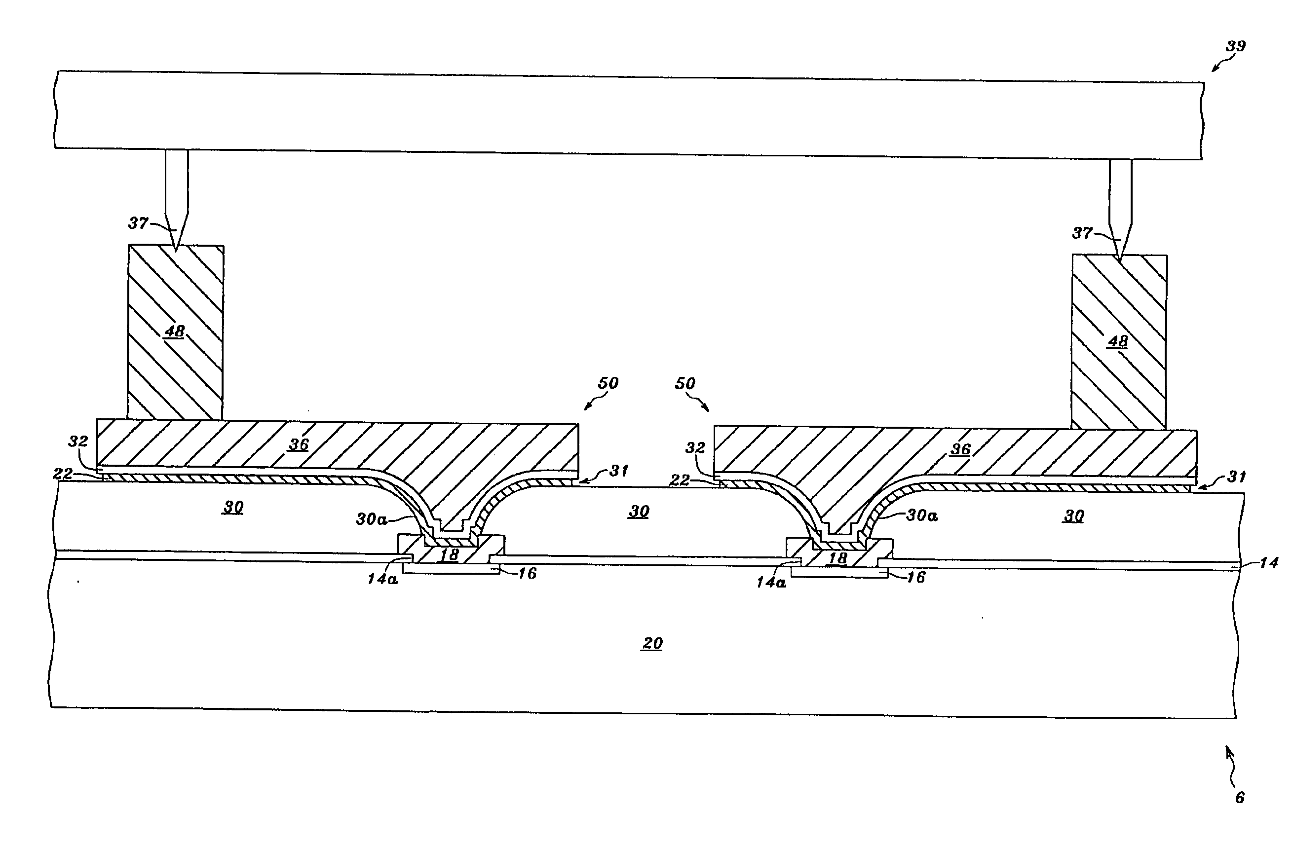
[0049]Referring to FIG. 2A, a titanium-tungsten-alloy layer 22 having a thickness of between 0.03 and 0.7 μm, and preferably of between 0.03 and 0.35 μm, can be formed on the passivation layer 14 and on the pads 16 exposed, respectively, by the openings 14a. Only one of the pads 16 and only one of the openings 14a are shown. For example, the titanium-tungsten-alloy layer 22 having a thickness of between 0.02 and 0.5 μm can be sputtered on the passivation layer 14 and on the pads 16, principally made of aluminum, exposed, respectively, by the openings 14a. Alternatively, the titanium-tungsten-alloy layer 22 having a thickness of between 0.02 and 0.5 μm can be sputtered on the passivation layer 14 and on the pads 16, principally made of copper, exposed, respectively, by the openings 14a. The titanium-tungsten-alloy layer 22 is treated as an adhesion / barrier layer to prevent the occurrence of interdiffusion between metal layers and to provide good adhesion between the metal layers.

[005...

embodiment 2

[0084]Referring to FIG. 3A, after the step shown in FIG. 2B, a photoresist layer 26, such as positive-type photoresist layer, having a thickness of between 10 and 35 micrometers is spin-on coated on the seed layer 24. Referring to FIG. 3B, the photoresist layer 26 is patterned with the processes of exposure and development to form multiple openings 26a in the photoresist layer 26 exposing the seed layer 24. A 1× stepper or 1× contact aligner can be used to expose the photoresist layer 26 during the process of exposure.

[0085]For example, the photoresist layer 26 can be formed by spin-on coating a positive-type photosensitive polymer layer having a thickness of between 10 and 35 μm on the seed layer 24, then exposing the photosensitive polymer layer using a 1× stepper or 1× contact aligner with at least two of G-line having a wavelength ranging from 434 to 438 nm, H-line having a wavelength ranging from 403 to 407 nm, and I-line having a wavelength ranging from 363 to 367 nm, illumina...

embodiment 3

[0111]In the present invention, multiple metal traces can be formed over the passivation layer 14. The process of forming the metal traces and testing the semiconductor wafer 6 will be illustrated in FIGS. 4A-4V.

[0112]One of the metal traces can be a redistributed metal trace to redistribute input or output positions. The redistributed metal trace is over the passivation layer 14 and on a first metal pad connected to the metallization structure, wherein the first metal pad may be a copper pad exposed by the opening 14a in the passivation layer 14, an aluminum pad exposed by the opening 14a in the passivation layer 14 or a metal cap 18 on a copper pad exposed by the opening 14a in the passivation layer 14. The redistributed metal trace comprises a second metal pad over the passivation layer 14, and the position of the second metal pad from a top perspective view is different from that of the first metal pad, to which the redistributed metal trace is connected. In a chip probing (CP) ...


PUM


Abstract

A method for fabricating and testing a wafer includes forming metal traces with metal pads, wherein forming the metal traces include forming a TiW layer on a passivation layer and on pads, next forming a seed layer on the TiW layer, next forming a photoresist layer on the seed layer, next forming a metal layer on the seed layer exposed by openings in the photoresist layer, next removing the photoresist layer, next removing the seed layer not under the metal layer, and then etching the TiW layer not under the metal layer with an etchant containing H2O2 at a temperature of between 35 and 50° C., or with an etchant containing H2O2 and with ultrasonic waves applied to the etchant, next contacting probe tips of a probe card with some of the metal pads, next cleaning the probe tips until repeating the step of contacting the probe tips with some of the metal pads at greater than 100 times, and then after cleaning the probe tips, repeating the step of contacting the probe tips with some of the metal pads.

Description

[0001]This application claims priority to U.S. provisional application No. 60 / 868,353, filed on Dec. 4 2006, which is herein incorporated by reference in its entirety.BACKGROUND OF THE INVENTION[0002]1. Field of the Invention[0003]The invention relates to a method for forming and testing a semiconductor wafer, by which the frequency of cleaning test probes is significantly reduced, and, more specifically, to a method for forming and testing a semiconductor wafer, by which the residual of metal oxide remaining on metal pads of the semiconductor wafer can be reduced, and the chance of the residual stuck onto the test probes can be diminished.[0004]2. Brief Description of the Related Art[0005]Titanium-tungsten alloy is one of barrier-type metals treated as an adhesion / barrier layer to prevent the occurrence of interdiffusion in semiconductor connector. Titanium-tungsten film, of 10% Ti and 90% W by weight, is layered onto a substrate under a sputtered gold film as a seed layer for foll...

Claims


Application Information

Patent Timeline
IPC IPC(8): H01L21/66
CPCH01L22/22H01L2224/02166H01L24/05H01L2924/1305H01L2924/00H01L2924/14
Inventor LIN, MOU-SHIUNGLIN, SHIH-HSIUNG
Owner QUALCOMM INC
Why Eureka
Try Eureka