

Semiconductor light emitting device and method for fabricating same
- Summary
- Abstract
- Description
- Claims
- Application Information
AI Technical Summary
Benefits of technology
Problems solved by technology
Method used
Image

Examples
example 1
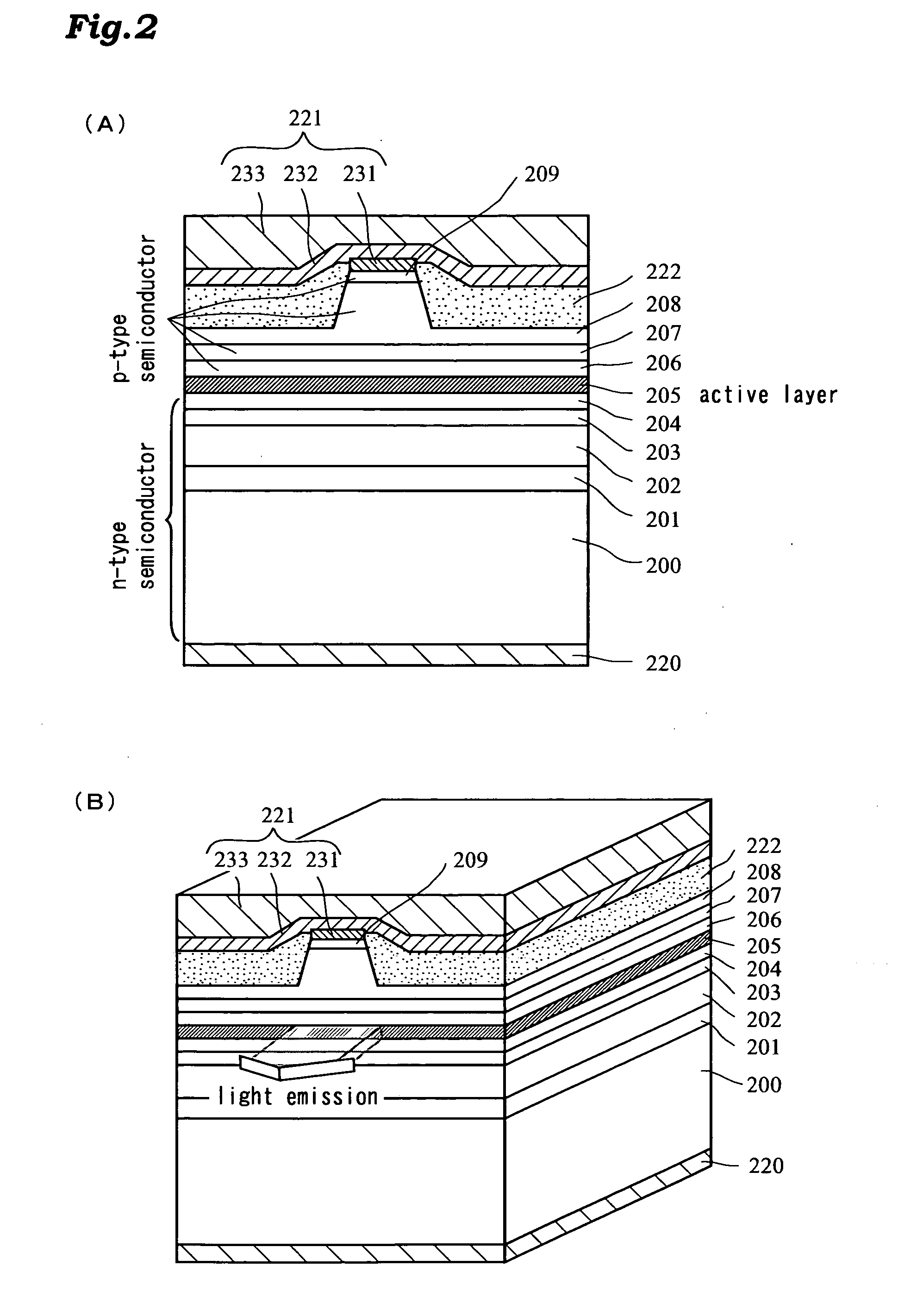
[0051]FIG. 2(A) is a schematic cross sectional view of a semiconductor laser element used in a semiconductor laser device according to example 1 of the present invention.
[0052]An insulation layer 222 is provided on the periphery of a protruding portion of a ridge-stripe structure to form a current-confined-path structure that has one electrode electrically connected only to the top of the protruding portion, thereby limiting part in which current passes. The current-confined-path structure enables an approximate control of the spot shape of emitted light. The insulation layer 222 contains hydrogen atoms at a concentration of 1×10¹⁷ / cm3 or more. The width of the protruding portion of the ridge-stripe structure is approximately 1.6 μm, and the length of the resonator is 600 μm. The element is subjected to AR (anti-reflective) coating on the front surface and HR (high reflection) coating on the rear surface.
[0053]P-type conductive layers are doped with, as a dopant, magnesium (Mg) at a...
example 2
[0080]A method for fabricating the nitride semiconductor laser device according to the present invention, and an assembly apparatus will be described.
[0081]Referring to FIG. 10, the assembly apparatus has a front chamber 101 and a working chamber 102. The front chamber 101 enables a necessary member for assembly to be introduced into the working chamber 102 without opening the working chamber 102 to atmosphere. To this end, the front chamber 101 has a mechanism 103 for introducing a purging gas. The working chamber 102 has therein an assembly mechanism 104 for assembling the nitride semiconductor laser device, thereby enabling assembly work in an externally-isolated sealed space. Between the front chamber 101 and the working chamber 102, there is transfer means (not shown) for transferring the necessary member for assembly. The front chamber 101 and the working chamber 102 are intercepted by a door 109.
[0082]The working chamber 102 also has: a vacuum mechanism 105 for making the in ...
PUM
 Abstract
Description
Claims
Application Information