Light emitting devices with a zinc oxide thin film structure

a thin film, zinc oxide technology, applied in semiconductor devices, basic electric elements, electric devices, etc., can solve the problems of hampered development of zno light emitters, unsuitable free-exciton light emission, and high price of refined form of indium, so as to minimize the concentration of native intra-crystal defects, promote grain growth, and increase the probability of free excitons

Inactive Publication Date: 2008-07-10
GROUP IV SEMICON
View PDF6 Cites 9 Cited by
  • Summary
  • Abstract
  • Description
  • Claims
  • Application Information

AI Technical Summary

Benefits of technology

[0020]f) baking the film to fully crystallize the film, promote grain growth, and minimize the concentration of native intra-crystal defects, thereby substan...

Problems solved by technology

In comparison, the low free-exciton binding energy in GaN, i.e. 25 meV, results in the free-excitons “boiling” apart at or below room temperature, making GaN unsuitable for free-exciton light emission.
Indium-tin oxide (ITO) is currently the industry standard for TCO material in flat panel displays, solar cells, etc; however, the global supply of indium metal is limited, thereby causing the price for the refined form of indium to be considerably higher than zinc, e.g. US$700/kg cf. for indium compared to US$4.00/kg for Zn, as of December 2006.
The required material properties for producing ZnO films suitable a...

Method used


Image

  • Light emitting devices with a zinc oxide thin film structure
  • Light emitting devices with a zinc oxide thin film structure
  • Light emitting devices with a zinc oxide thin film structure

Examples


Embodiment Construction

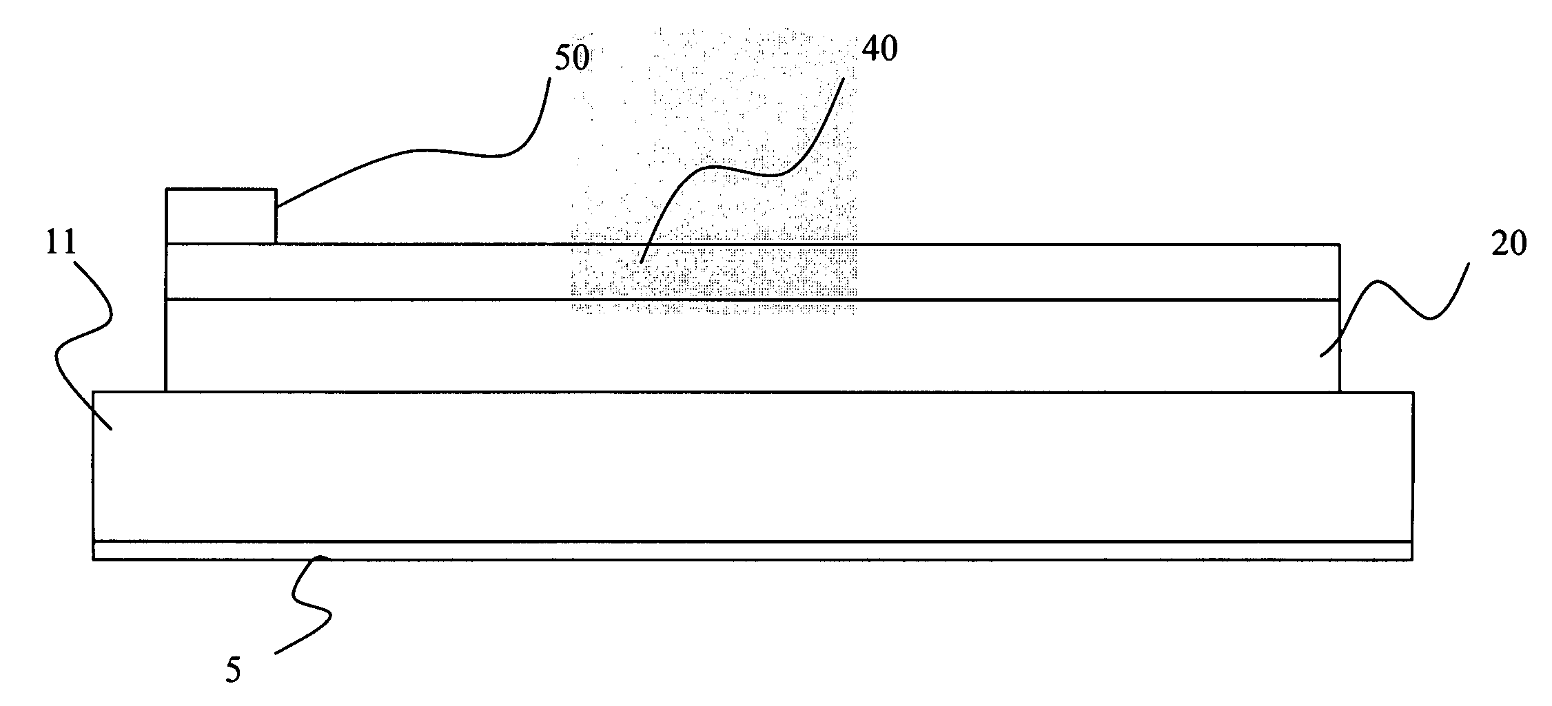
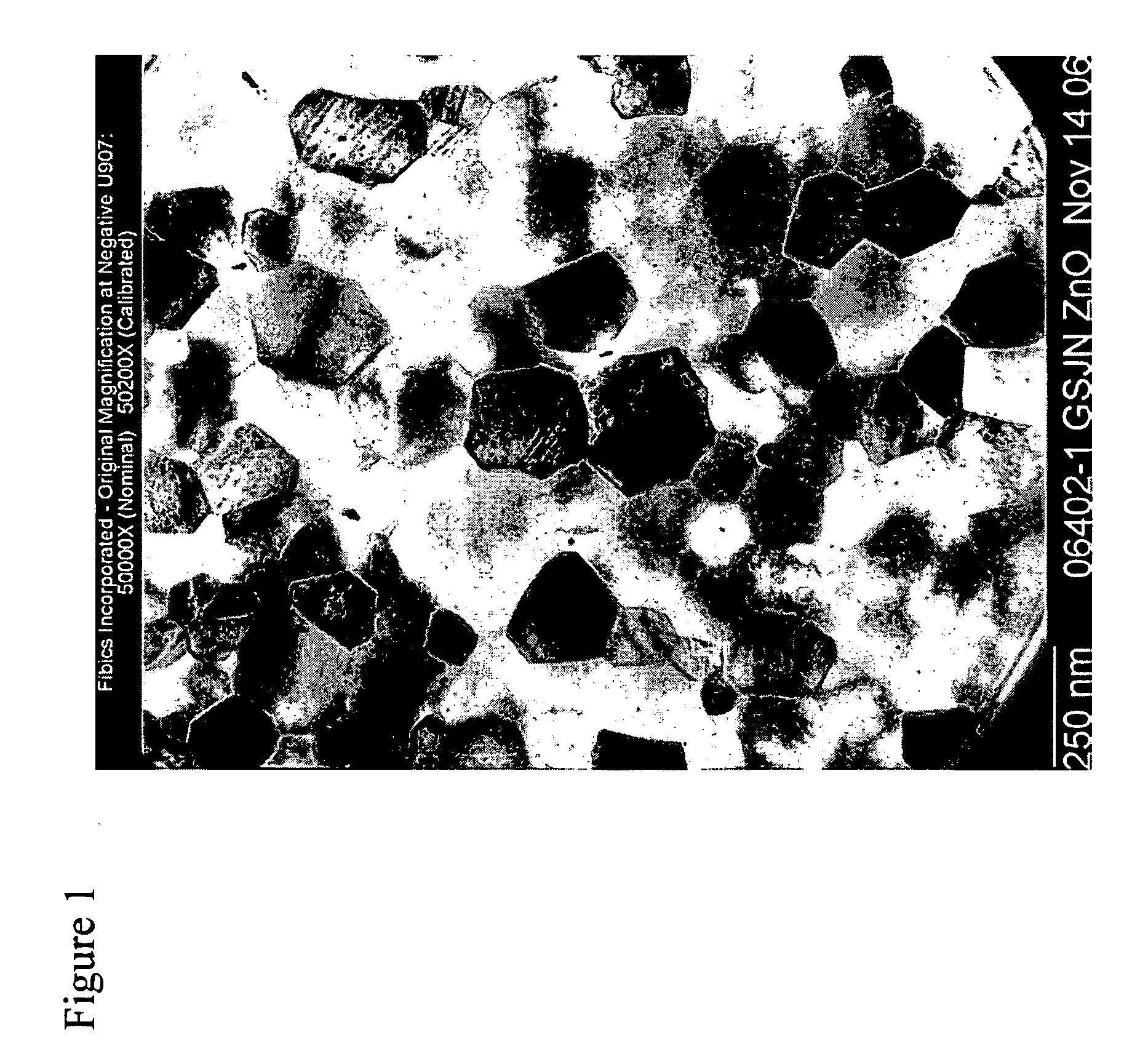
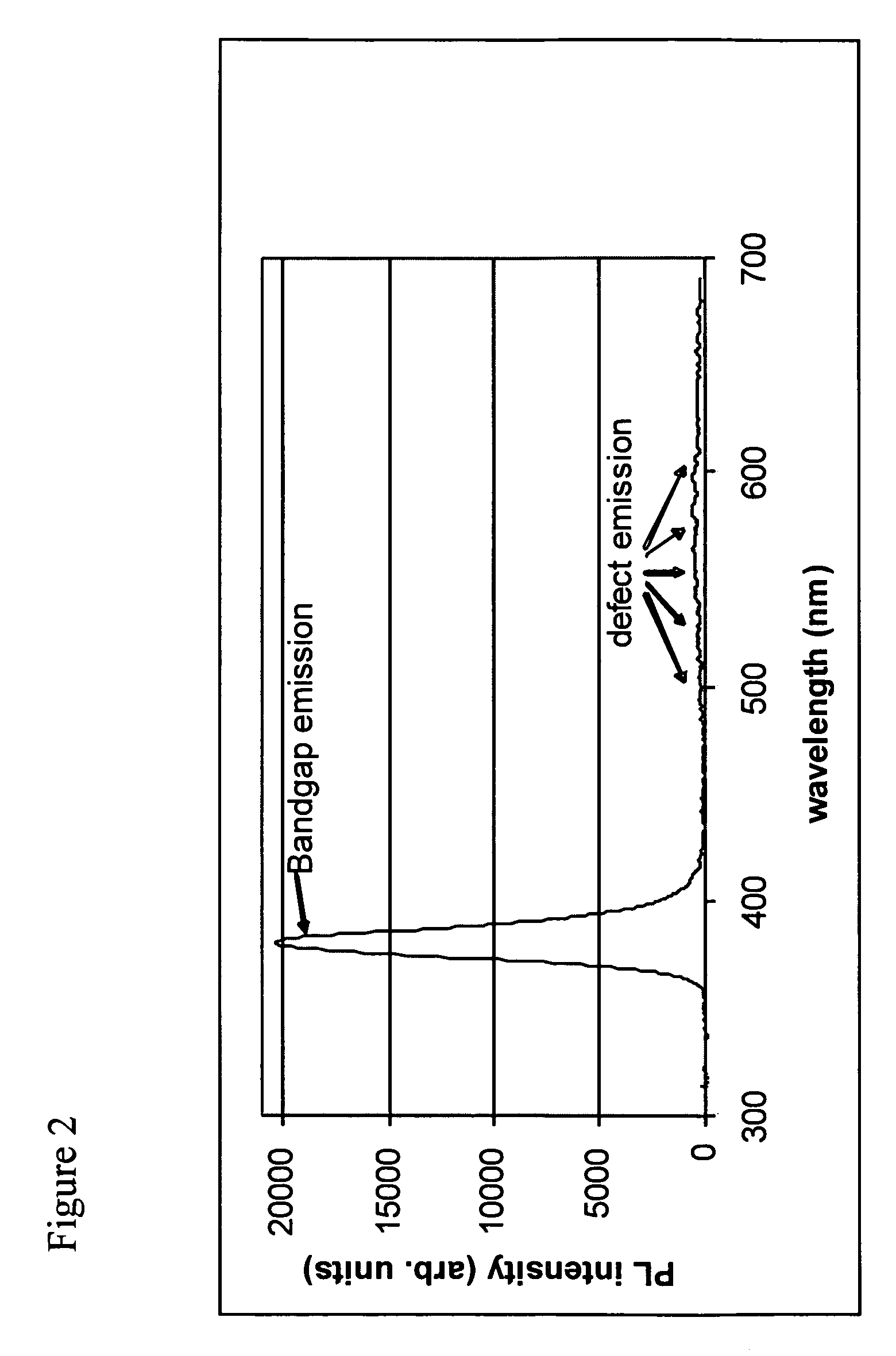
[0033]The present invention relates to direct-bandgap, semiconductor-material, thin films, such as zinc oxide (ZnO) or ZnO alloyed, e.g. with beryllium, cadmium and magnesium, for use in producing efficient electro-luminescent devices by enhancing the intensity of the bandgap light emission compared to the deep level (defect) light emission typically observed to be dominant in most direct-bandgap semiconductor devices, by providing a dopant with high concentrations of free-exciton binding centers. Specifically, the present invention is achieved by using process conditions for simultaneously satisfying all of the following materials requirements during fabrication of the electro-luminescent device or the optically active layer:

[0034](1) minimizing the concentration of point defects within the direct-bandgap, semiconductor material, e.g. ZnO, optically active layer (film), comprising a single crystal or polycrystalline grains, in particular the native defects involving vacancies and i...


PUM


Abstract

The present invention relates to a sol-gel deposition/heat treatment process, which consistently produces polycrystalline direct bandgap semiconductor, e.g. ZnO, thin films exhibiting a photo luminescent (PL) spectrum at room temperature that is dominated by a single peak, e.g. in the ultraviolet part of the spectrum, in which the PL intensity of the bandgap emission is more than approximately 40 times greater than any deep-level defect emission peak or band. The present invention incorporates such direct bandgap semiconductor, e.g. ZnO, polycrystalline thin films produced by the method of the present invention into electro-luminescent devices that exhibit similarly high ratios of bandgap/deep-level defect emission intensity.

Description

CROSS-REFERENCE TO RELATED APPLICATIONS[0001]The present invention claims priority from U.S. Patent Application No. 60 / 884,266 filed Jan. 10, 2007, which is incorporated herein by reference.TECHNICAL FIELD[0002]The present invention relates to light-emitting semiconductor thin film device, and in particular to direct-bandgap semiconductor material, such as a zinc-oxide (ZnO) or a ZnO alloy, with a dopant for populating the direct bandgap semiconductor material with free-exciton binding centers in concentrations above native defect concentration.BACKGROUND OF THE INVENTION[0003]Zinc oxide (ZnO) is a multifunctional semiconductor material which has been used in various areas, including phosphors, piezoelectric transducers, surface acoustic wave devices, gas sensors, and varistors. With a band gap of approximately 3.3 eV, ZnO is similar to that of Gallium Nitride (GaN), but with a higher free-exciton binding energy of 60 meV, compared to 25 meV for GaN, thereby favoring efficient free-...

Claims


Application Information

Patent Timeline
IPC IPC(8): H01L33/00
CPCC09K9/02
Inventor RIOUX, BRIANNOEL, JEAN-PAUL
Owner GROUP IV SEMICON
Why Eureka
Try Eureka