Optical proximity correction improvement by fracturing after pre-optical proximity correction

Inactive Publication Date: 2008-07-10
IBM CORP
17 Cites 12 Cited by

AI-Extracted Technical Summary

Problems solved by technology

The resolution of an exposure system is limited by the contrast of the projected light image, that is the intensity difference between adjacent light and dark features.
Sub-wavelength lithography, where the size of printed features is smaller than the exposure wavelength, places a tremendous burden on the lithographic process.
Distortions of the intended images inevitably arise, primarily because of the nonlinearities of the imaging process and the nonlinear response of the photoresist.
The former type of distortion can cause variations in circuit timing and yield, whereas the latter can lead to poor current tolerances and higher probabilities of electrical failure.
Moreover, optical proximity effects ar...

Abstract

A method for fabricating a mask used to make integrated circuits is provided using an improved OPC process whereby a pre-fracturing OPC process is performed on the target design of the integrated circuit. The pre-fractured OPC design is then fractured and a post-fracturing OPC process performed to make the final mask. Either rule-based OPC or model-based OPC processes can be used for both of the OPC steps or each step can be either side-based or model-based OPC.

Application Domain

Originals for photomechanical treatmentComputer aided design +2

Technology Topic

Integrated circuitOptical proximity correction +1

Image

  • Optical proximity correction improvement by fracturing after pre-optical proximity correction
  • Optical proximity correction improvement by fracturing after pre-optical proximity correction
  • Optical proximity correction improvement by fracturing after pre-optical proximity correction

Examples

  • Experimental program(1)

Example

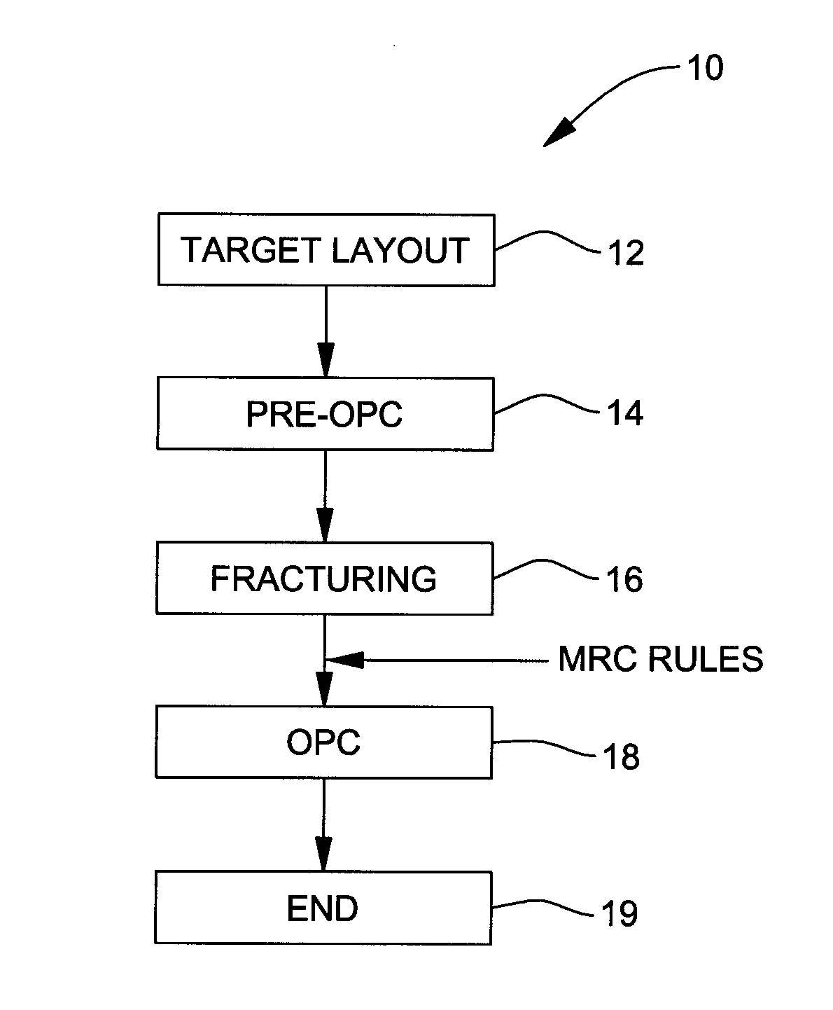
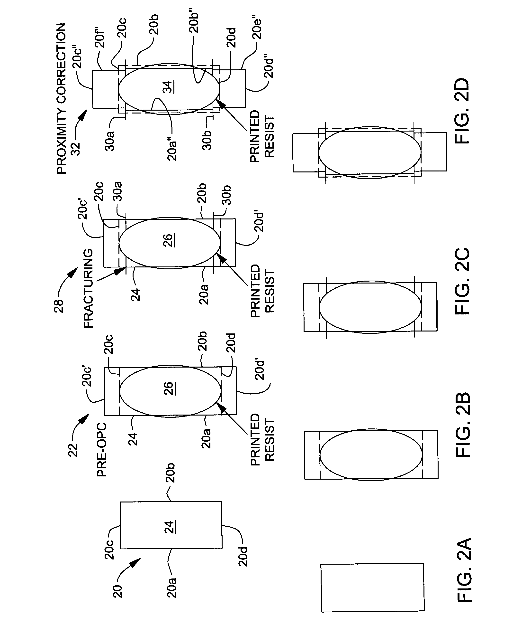
[0036]In describing the preferred embodiment of the present invention, reference will be made herein to FIGS. 1-4C of the drawings in which like numerals refer to like features of the invention.
[0037]Accurate definition of mask patterns having line widths less than the wavelength of light is generally implemented using OPC (optical proximity correction), a collection of techniques for correcting beforehand the shape of mask patterns, to allow for pattern deformations on the wafer caused by the so-called optical proximity effect. This collection of OPC techniques is also called PPC (process proximity effect correction). A typical OPC tool of this type is rule-based OPC.
[0038]Rule-based OPC is implemented as follows: a test-use mask pattern is prepared using test patterns representing all patterns that are permitted by design. The test patterns are transferred through the mask pattern onto the wafer for pattern etching, whereby a test-use wafer is produced.
[0039]The pattern geometry on the test-use wafer is then measured. The measured data, together with design data from the test-use mask pattern, are used as a basis for generating rule-based OPC, i.e., a collection of design rules for determining bias data to be added to mask pattern design data. The mask pattern is then corrected using the rule-based OPC. The correction takes place at a mask pattern layout stage in the CAD process. The mask fabricated through OPC is called the OPC mask.
[0040]Apart from rule-based OPC, there is another set of corrective techniques called model-based or simulation-based OPC.
[0041]This type of proximity effect correction involves generating a simulation-based OPC model (also called a kernel or a process model) that represents a pattern transfer process allowing for the optical proximity effect based on the measurements of a limited number of test patterns prepared beforehand. Differences in shape between the mask pattern and the pattern geometry transferred through the mask pattern onto the wafer are simulated by the simulation-based OPC model. The results of the simulation are used to correct the mask pattern. Model-based OPC is calibrated using physical structures just as much as rule-based OPC. The model is a physical model but there is always a fitting component that comprehends resist effects, process effects, and the like.
[0042]OPC is a well-known technique used in the fabrication of electronic components such as integrated circuits and need not be detailed herein. A number of U.S. patents describe OPC including U.S. Pat. Nos. 5,682,323; 6,854,104; 6,829,380; 6,928,636; and 6,934,929. These patents are hereby incorporated by reference.
[0043]Referring first to the prior art FIG. 3 and FIGS. 4A-4C, the prior art method is shown and how the prior art method forms a mask feature for generating a target feature on the semiconductor device.
[0044]In the flow sheet of FIG. 3 shown generally as numeral 100, a target layout is determined in step 102. The target is fractured in step 104 and OPC is performed under consideration of MRC rules in step 106. The method ends in step 108.
[0045]In FIG. 4A two adjacent target features are shown generally as numeral 110 with the target having sides 110a, 110b, 110c, and 110d. The sides define a target feature 112. The target feature 112 is the target that the semiconductor designer wants on the chip.
[0046]In FIG. 4B the oval-shape 114 indicates the approximate printing on the resist without an OPC procedure. The target is fractured shown as lines 116a and 116b.
[0047]In step 4C OPC is performed on the fractured feature of FIG. 4B. The target feature is shown by the dotted lines and the mask feature generated by the OPC procedure as the solid rectangular lines, numerals 110a′-110f′. The oval-shape 118 indicates the approximate printing on the resist after the OPC procedure and it should be noted that the oval shape does not come close to the target in length because the OPC was prevented from moving the mask edges because of MRC rules.
[0048]FIG. 1 shows a flow chart of the subject invention generally as numeral 10. In step 12 a target layout is prepared and in step 14 a pre-OPC procedure is performed on the target layout. The pre-OPC procedure is performed before any fracturing of the target layout. In step 16 fracturing is then performed and in step 18 the OPC procedure is performed. The process ends in step 19.
[0049]Referring now to FIGS. 2A-2D the method of the invention can be shown. InFIG. 2A a target layout is shown generally as numeral 20 and comprises adjacent rectangular shapes having sides 20a, 20b, 20c, and 20d. The sides enclose a target area 24.
[0050]In FIG. 2B the results of a pre-OPC procedure are shown as numeral 22. The pre-OPC procedures forms a pre-OPC shape 22, bounded by solid lines 20a, 20b, and 20c′ and 20d′. This would form a printed oval shape 26 which indicates the approximate shape of the photoresist on the wafer after pre-OPC if the solid line shape was formed on a mask and printed. As can be seen the image is still not as desired since it is too wide at the center of the target. Note also that the mask design 22 has been lengthened so that the ends are now 20c′ and 20d′. The pre-OPC procedure was performed using model-based OPC. Calibre solid by Mentor Graphics Corporation was used.
[0051]FIG. 2C shows the fracturing of the pre-OPC geometries generally as numeral 28. The target feature is fractured along lines 30a and 30b and was performed based on rules. For example, fracturing is performed a certain distance, e.g., 40 nm from a corner along a long side and no fracturing on a short side (line end). Fracturing is typically done within the OPC tool such as for example, using Calibre sold by Mentor Graphics Corporation, to do both fracturing and OPC.
[0052]FIG. 2D shows the final mask layout which achieves good printing in the resist and does not run into mask rule checks of the OPC procedure. Thus, the target layout on the mask is now defined by the solid rectangular lines 20a″-20f″. The target feature is still shown by dotted lines 20a-20d. The final layout shown by oval 34 is the approximate shape of the photoresist on the wafer obtained by the mask feature defined by the solid lines 20a″-20f″. This printed feature is closer to the target design obtained by the prior art method shown by FIGS. 3 and 4A-4C. The post-OPC procedure was performed using model-based OPC using Calibre.
[0053]While the present invention has been particularly described, in conjunction with a specific preferred embodiment, it is evident that many alternatives, modifications, and variations will be apparent to those skilled in the art in light of the foregoing description. It is therefore contemplated that the appended claims will embrace any such alternatives, modifications, and variations as falling within the true scope and spirit of the present invention.

PUM

no PUM

Description & Claims & Application Information

We can also present the details of the Description, Claims and Application information to help users get a comprehensive understanding of the technical details of the patent, such as background art, summary of invention, brief description of drawings, description of embodiments, and other original content. On the other hand, users can also determine the specific scope of protection of the technology through the list of claims; as well as understand the changes in the life cycle of the technology with the presentation of the patent timeline. Login to view more.
Why Eureka
Try Eureka