
Method of manufacturing semiconductor chip assembly with sacrificial metal-based core carrier

Inactive Publication Date: 2008-08-07
BRIDGE SEMICON
View PDF0 Cites 51 Cited by
  • Summary
  • Abstract
  • Description
  • Claims
  • Application Information

AI Technical Summary

Benefits of technology

[0041]An advantage of the present invention is that the semiconductor chip assembly can be manufactured conveniently on a solid supporting panel to improve dimensional stability and handling issues.
[0042]Another advantage of the present invention is that the metal-based core carrier provides the critical flatness, hardness and rigidity support during flip chip thermo-compression bonding, there by enhancing the bond strength of the chip to the build-up substrate.
[0043]Another advantage of the present invention is that the metal-based core carrier provides the important hardness and high thermal conduction during flip chip thermo-sonic bonding, thereby enhancing the bond strength of the chip to the build-up substrate.
[0044]Yet another advantage of the present invention is that the assembly made by this method is characterized by high chip-to-substrate bonding strength. The unique metallurgical gold-gold bonding provides superior bonding strength due to the monolithic structure of the gold material formed by the thermo-sonic bonding between gold stud bond and gold pad. The metal-based core carrier provides high thermal conductivity to facilitate thermo-sonic bonding; and, the interconnection maintains low contact resistance, sustains high current flow, and provides superior high frequency performance (low inductance).
[0045]Another advantage of the present invention is that the connection joint can be made from a wide variety of materials and processes, thereby making advantageous use of mature connection joint technologies in a unique and improved manufacturing approach.
[0046]Another advantage of the present invention is that as the encapsulant can be provided before the metal-based core carrier is etched and removed, the carrier provides the mechanical support and protection for the chip and the routing line during assembly before the metal base is etched.

Problems solved by technology

While the conventional build-up substrate has tremendous advantages for high performance chips, its technical and reliability limitations are significant.
As the wiring density and the through holes dimension of the core are significantly coarser than those in the build-up layers, the core can only provide limited wiring functions for the connection means for the front and back side of the build-up layers.
As a result, even though flip chip terminal pitches can be easily accommodated by the wiring capability in the build-up layers, the through-hole in the core actually imposes a severe restriction on the wiring capability of the second build-up layer.
In addition, the plated through holes in the core often destroys the integrity of the voltage layer as it increases capacitance loss and electrical noise.
Besides the wiring restriction problem associated with core laminate, the local and global thermal expansion coefficient (CTE) mismatches of the silicon and substrate materials will induce large thermal stress and strain.
As a result, a weak solder joint connection between the semiconductor package and the circuit board will incur during next level board assembly.
Thermal mismatch of these materials also induce serious warping and handling problems and thus greatly affect the package's manufacturing yield.
As such, the manufacturing processes and material lay-up for a semiconductor package should be carefully designed since not only the electrical and thermal performances of the packaging system can be strongly affected, the degradation of the physical mechanical structure of the package can also cause a serious reliability problem and have an adverse impact on the manufacturing yield.
However, such core-less substrate suffers a serious problem in losing the rigidity support that packaging processes normally require.
Furthermore, the deformation of sheets and poor co-planarity control of such ultra-thin substrate would cause dimension and alignment issues during chip assembly, as such, low manufacturing yield and many reliability-related problems would make this approach un-favorable.
A drawback to this approach is that, when the wire bonder forms the gold ball on the pad, it applies substantial pressure to the pad that might destroy an active circuitry beneath the pad.
In addition, gold from the pin can be dissolved into the solder to form a gold-tin intermetallic compound which mechanically weakens the pin and therefore reduces reliability.
While the posts and the flexible substrate can give a certain amount of compliancy to the structure, this technique encounters many difficulties in controlling dimensional stability prior to and during the assembly steps.
The protruded pins would cause tremendous handling issues during assembly and induce unwanted bending and shorting after assembly and hence have an adverse effection the assembly process, making this approach a tedious and less than desirable assembly solution from a manufacturing point of view.
Hence, the prior arts do not fulfill all users requests on actual use.

Method used


Image

  • Method of manufacturing semiconductor chip assembly with sacrificial metal-based core carrier
  • Method of manufacturing semiconductor chip assembly with sacrificial metal-based core carrier
  • Method of manufacturing semiconductor chip assembly with sacrificial metal-based core carrier

Examples


Embodiment Construction

[0065]The following descriptions of the preferred embodiments are provided to understand the features and the structures of the present invention.

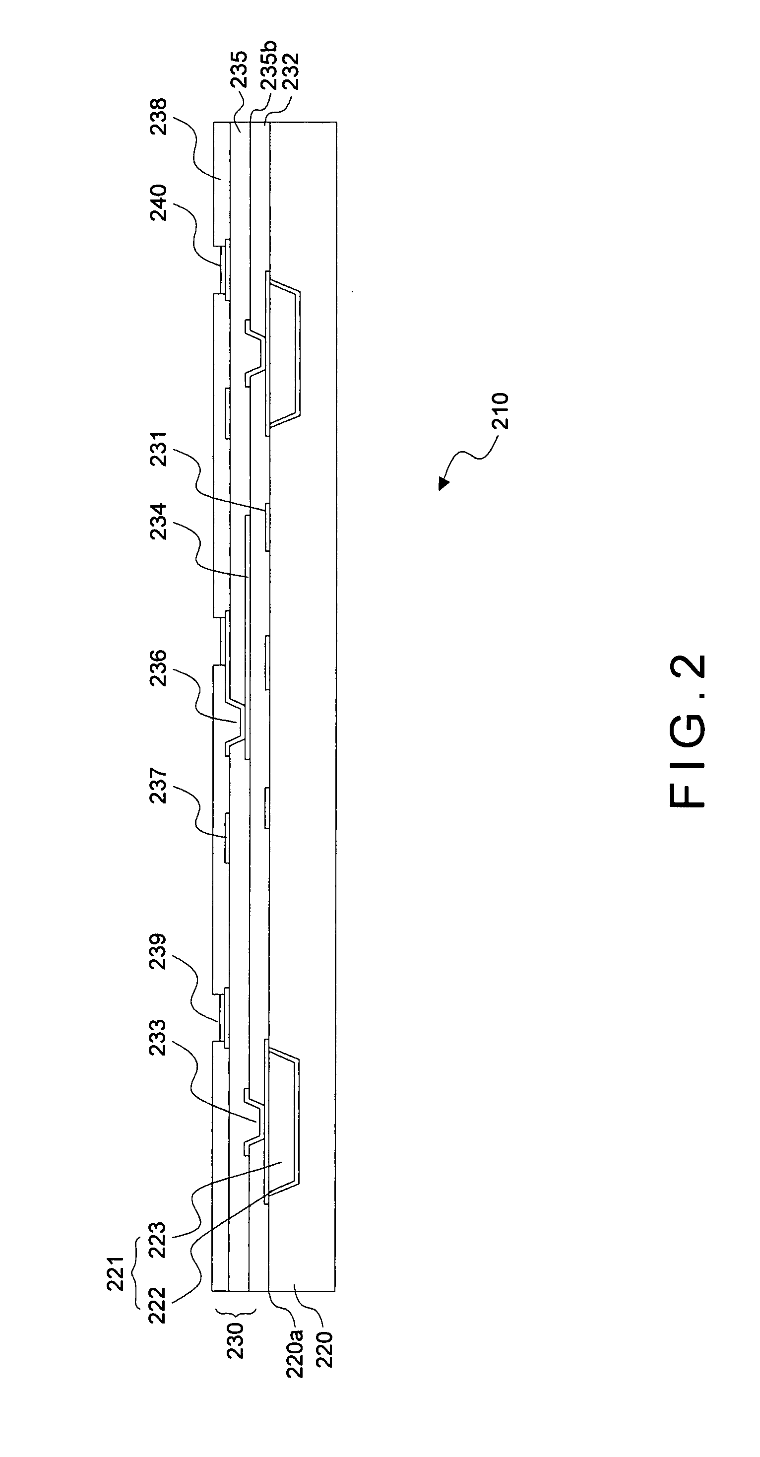
[0066]Please refer to FIG. 2, which is a cross sectional view showing a build-up substrate according to a preferred embodiment of the present invention.

[0067]As shown in the figure, the present invention is a build-up substrate 210 with a metal-based core carrier 220 where the build-up layers are deposited on the first surface 220a of the metal-based core carrier 220. The metal-based core carrier 220 is typically made of a copper plate or other materials, such as aluminum or metal alloys, that can be chemically etched or mechanically removed.

[0068]For ease of reference, throughout the description of the present invention, the metal-based core carrier 220 may be referred to as a metal-based core carrier for convenience or as a metal base in some instances when it does not perform the function of a carrier, and is sacrificed through etching....


PUM


Abstract

A method of making a semiconductor chip assembly is disclosed. The semiconductor chip assembly is made by attaching a semiconductor chip to a multi-layer build-up substrate with a metal-based core carrier. The build-up substrate layers provide routing functions while the metal-based core carrier provides critical mechanical support for the semiconductor assembly. The metal-based core carrier is sacrificial and is eventually removed with the build-up substrate remaining.

Description

FIELD OF THE INVENTION [0001]The present invention relates to a semiconductor chip assembly technology; more particularly, relates to assembling an integrated circuit chip on a build-up substrate with a metal-based core carrier.DESCRIPTION OF THE RELATED ARTS [0002]Increased integrated circuit (IC) functionality, coupled with the challenges to achieve desired signal integrity and smaller form-factor has birthed a wide range of advanced packaging innovations including flip chip (FC) and chip-scale packaging (CSP). These technologies allow chip to be packed in a very dense area by using a high density interconnect (HDI) substrate to distribute I / O signals effectively from the IC to the board. The HDI substrate not only miniaturizes the foot print of a package, but also improves signal integrity, such as noise reduction, EMI radiation reduction, and low attenuation. A number of new processes have been evolved to provide HDIs and one of t he most popular is a group referred to as sequen...

Claims


Application Information

Patent Timeline
IPC IPC(8): H01L21/00
CPCH01L21/4846H01L21/563H01L2924/01327H01L2924/014H01L21/565H01L21/6835H01L23/3114H01L23/49811H01L23/49822H01L24/12H01L24/16H01L24/81H01L2221/68345H01L2221/68377H01L2221/68381H01L2224/13144H01L2224/16225H01L2224/73204H01L2224/81001H01L2224/81208H01L2224/81801H01L2924/01013H01L2924/01029H01L2924/01033H01L2924/01046H01L2924/01078H01L2924/01079H01L2924/01082H01L2924/14H01L2924/15311H01L2924/19041H01L2924/19043H01L2924/30105H01L2924/30107H05K3/205H05K3/4007H05K2201/0367H05K2203/0376H01L2924/01005H01L2924/01006H01L2924/01019H01L2924/01047H01L2924/0105H01L2924/01075H01L2924/00H01L2924/351H01L2924/181H01L2224/16237H01L2224/05573H01L2224/05568H01L2924/00014H01L2224/0554H01L2924/00012H01L2224/05599H01L2224/0555H01L2224/0556
Inventor LIN, CHARLES W.C.
Owner BRIDGE SEMICON
Learn More