Method and apparatus for measuring pattern dimensions

a circuit pattern and measurement method technology, applied in the direction of semiconductor/solid-state device testing/measurement, instruments, etc., can solve the problems of deteriorating measurement repeatability, difficult to reduce the s/n ratio by an image process without changing waveform, and degrading information of pattern shape and pattern dimensions, etc., to reduce the amount of electron radiation, reduce the damage to the pattern, and improve the repeatability of measurement

Inactive Publication Date: 2008-08-21
HITACHI HIGH-TECH CORP
View PDF2 Cites 26 Cited by
  • Summary
  • Abstract
  • Description
  • Claims
  • Application Information

AI Technical Summary

Benefits of technology

[0011]As described in the Background of the Invention, in the measurement using the electron microscopic image, the repeatability of measurement is secured by reducing the amount of radiation of electrons to reduce damage to the pattern and reducing an effect of reduction of an image S / N ratio by the amount of radiation of electrons using an image processing means such as smoothing. However, although the image processing means such as smoothing can reduce an effect of noise, it may degrade information of the pattern shape and dimensions of the pattern. FIGS. 4 and 5 show examples of deterioration of waveform information by a smoothing process and specifically show that an original SEM image waveform is greatly changed by the smoothing process.
[0014]In contrast, the smoothing process is effective in improving the measurement repeatability, but since the waveform variation occurring due to the smoothing process as shown in FIG. 4 or 5 deteriorates the pattern shape information, the use of such an image can not realize measurement with high accuracy in consideration of the sectional shape of the pattern, thereby making it difficult to realize measurement with high precision to meet a need of measurement high accuracy according to pattern size shrink.
[0015]It is therefore an object of the invention to realize high accurate measurement of pattern dimensions using electron microscopic image (SEM image) by reducing an effect of noise even in an image having a low S / N ratio, without deteriorating information on shape and dimensions of an original pattern. If the information on the shape and dimensions of the pattern can be obtained even in the image having the low S / N ratio, then it is possible to realize measurement of pattern dimensions with high accuracy without electron beam damage to the pattern.
[0016]To accomplish the above object, by calculating edge position deviations due to roughness of a pattern, correcting the calculated edge position deviations for signal waveforms, and averaging the signal waveform corrected edge position deviations, an average waveform having low noise at an average position is generated without degrading waveform shape information of edges. When measurement is carried out using the average waveform, it is possible to realize highly accurate measurement.
[0017]With this configuration, it is possible to realize fast and highly accurate CD-SEM measurement without electron beam damage. For even an image having a low S / N ratio, since 3-dimensional shape information of a pattern in the image can be detected with high sensitivity, it is possible to manage or control a semiconductor manufacturing process state such as pattern shape variation based on a result of pattern measurement of the invention. In addition, measurability in an image having a low S / N ratio allows reduction of time taken to acquire an image, thereby increasing throughput of pattern dimension measurement.

Problems solved by technology

However, although the image processing means such as smoothing can reduce an effect of noise, it may degrade information of the pattern shape and dimensions of the pattern. FIGS. 4 and 5 show examples of deterioration of waveform information by a smoothing process and specifically show that an original SEM image waveform is greatly changed by the smoothing process.
For this reason, when an averaging process in a longitudinal direction of a line as shown in FIG. 5 is performed, a signal waveform of an SEM image is deformed by an affect of this roughness, thereby making it difficult to reduce an S / N ratio by an image process without changing waveform.
−2┘, in the method of measuring dimensions in consideration of the sectional shape of the pattern, it is disclosed that the measurement repeatability is deteriorated when an S / N ratio of the target image to be measured is poor.
In contrast, the smoothing process is effective in improving the measurement repeatability, but since the waveform variation occurring due to the smoothing process as shown in FIG. 4 or 5 deteriorates the pattern shape information, the use of such an image can not realize measurement with high accuracy in consideration of the sectional shape of the pattern, thereby making it difficult to realize measurement with high precision to meet a need of measurement high accuracy according to pattern size shrink.

Method used


Image

  • Method and apparatus for measuring pattern dimensions
  • Method and apparatus for measuring pattern dimensions
  • Method and apparatus for measuring pattern dimensions

Examples


first embodiment

[0061]First, basic electron microscopic image processing of a pattern measuring method according to a first embodiment of the invention will be described with reference to FIGS. 1 to 3.

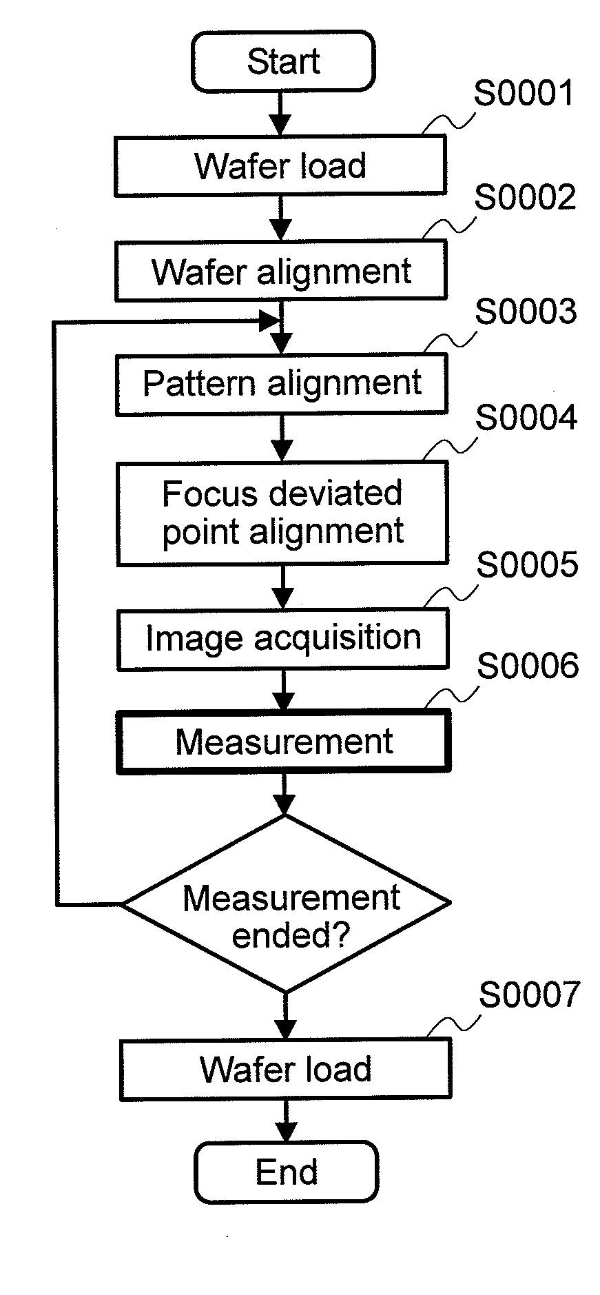
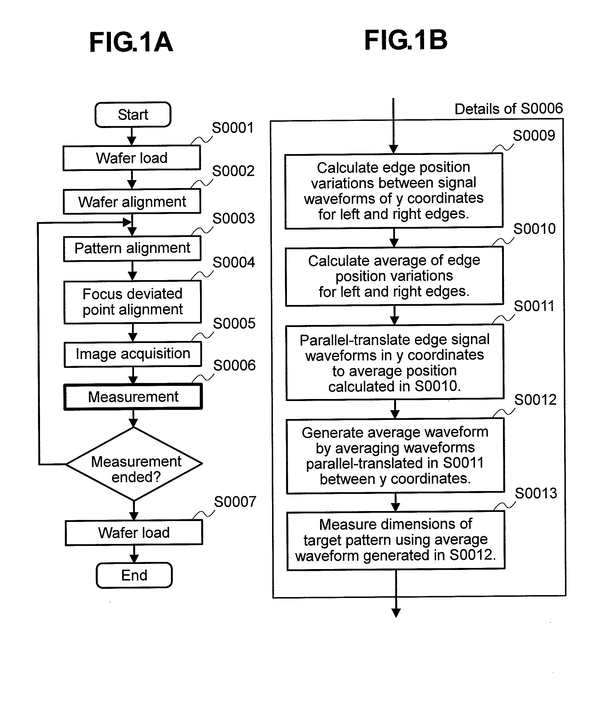
[0062]FIG. 1A shows one example of measurement procedure using a SD-SEM in the pattern measurement method of the invention. FIG. 1B is a flow chart illustrating details of Step S0006 in the flow chart of FIG. 1A.

[0063]Actual measurement is carried out in an order shown in FIG. 1A. First, a wafer is loaded into an apparatus in a similar way in normal SD-SEM measurement (S0001), and a position of a pattern on the wafer is corrected by wafer alignment (S0002). Next, a stage is moved near the pattern to be measured, and accurate positioning using preset neighboring patterns (S0003) and image quality is adjusted by focus and astigmatism / focus adjustment (S0004). Thereafter, a SEM image of the pattern to be measured is acquired (S0005) and then measurement for the pattern is carried out (S0006).

[0064]FIG. 1...

second modification

of First Embodiment

[0094]In a second modification, like the first modification, another method of performing an edge position aligning process with high precision in consideration of roughness will be described with reference to FIGS. 13 and 14.

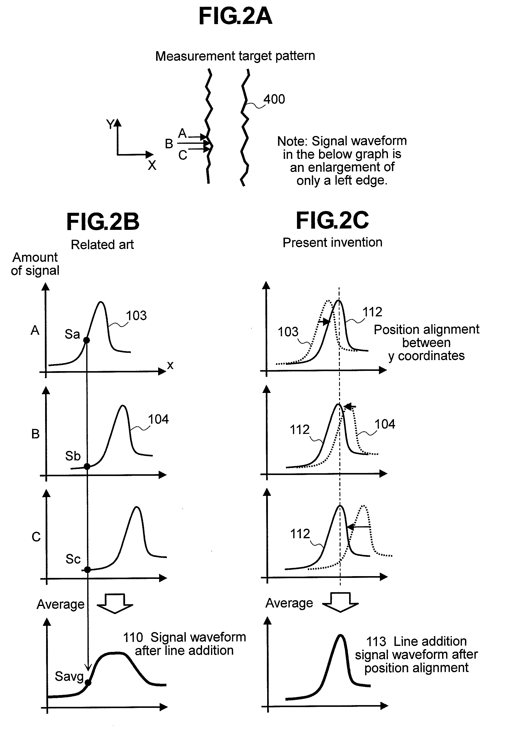
[0095]In the second modification, when position deviations between signal waveforms of edge portions are calculated, a signal waveform having a high S / N ratio is separately generated as a template for position alignment. In the second modification of the first embodiment shown in FIG. 14, a line addition process is performed in advance within a range having no effect on a waveform shape. FIG. 13 shows a frequency characteristic of general semiconductor line pattern wiring width deviation as disclosed in Non-Patent Document 6. As can be seen from FIG. 13, the wiring width deviation has a relatively large amplitude in a low frequency domain while having a suddenly decreasing amplitude in a high frequency domain. This locates at a relatively nea...

third modification

of First Embodiment

[0100]In a third modification, like the first and second modifications, another method of performing an edge position aligning process with high precision in consideration of roughness will be described with reference to FIGS. 15 and 16.

[0101]In the third modification of the first embodiment as shown in FIGS. 15 and 16, an affect of noises is reduced by applying a smoothing filter before calculating edge position deviation. Since the image smoothing process deforms a signal waveform, as shown in FIG. 5, this smoothing process requires special care in application to an image to be measured, however, if the same smoothing process is applied to both of waveforms whose position deviations are compared to each other, there occurs no particular problem.

[0102]FIG. 15 shows a relationship between an edge position in a pattern edge portion and pixels of the image. A right gray portion denotes a line pattern (line portion) and a left white portion denotes an underlying port...


PUM


Abstract

It is difficult for a material having low resistance to electron beam irradiation to obtain an electron microscopic image having a high S / N ratio. A conventional image smoothing process can improve stability of measurement, but this process has a problem of measurement errors for absolute values, reduction of sensitivity, deterioration of quality of cubic shape information and the like. In the present invention, by performing an image averaging process without deteriorating cubic shape information of a signal waveform in consideration of dimension deviation of a measurement target pattern, measurement stability is compatible with improvement of precision and sensitivity. Accordingly, it is possible to realize measurement of pattern dimensions and shapes with high precision and control of a highly sensitive semiconductor manufacturing process using the measurement.

Description

CLAIM OF PRIORITY[0001]The present application claims priority from Japanese application serial no. JP2007-040190, filed on Feb. 21, 2007, the content of which is hereby incorporated by reference into this application.BACKGROUND OF THE INVENTION[0002]1. Field of the Invention[0003]The present invention relates to a method and system for measuring dimensions of a shape of a circuit pattern, which is formed on a wafer, using an electron microscopic image of the circuit pattern in a process of manufacturing a semiconductor device.[0004]2. Description of Related Art[0005]Dimensions and shape of a multi-layered pattern formed on a wafer as a substrate are important factors having a great influence on performance of the semiconductor device in a manufacturing process of a semiconductor device. In particular, a wiring pattern including a transistor gate wiring has a strong connection with its wiring width and shape, and accordingly, it is very important to build a manufacturing process to ...

Claims


Application Information

Patent Timeline
Patent Type & Authority Applications(United States)
IPC IPC(8): G01B15/00
CPCG01B15/04G01N23/225H01J2237/2817H01L22/12Y10S430/143H01L2924/0002H01L2924/00
Inventor TANAKA, MAKISHISHIDO, CHIENAGATOMO, WATARU
Owner HITACHI HIGH-TECH CORP
Why Eureka
Try Eureka